PCB Capabilities
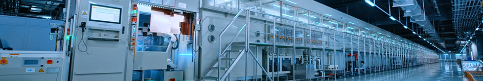
Panda PCB Group has invested in advanced PCB manufacturing equipment from Germany, Israel, Taiwan, and other regions. Our state-of-the-art facilities include vacuum pressing machines, vacuum etching lines, LDI automatic exposure machines, AOI automated optical inspection, laser drilling, laser trimming machines, six-axis CNC drilling and milling machines, automatic vertical electroplating systems, and resin hole-filling equipment, among others. Our factory employs unique interlayer alignment technology, advanced inspection techniques, and strict control processes to ensure the highest standards of PCB quality. We are committed to establishing an efficient, automated manufacturing and management production model, with the goal of becoming a leading and trustworthy high-end PCB manufacturer. |
 |
1 , Process Capabilities of Conventional PCB (FR4) :
Process |
Item |
PCB Process Capabilities |
|
Base Information |
Production Capabilities |
Layer count |
1-30 layers |
Bow and twist |
0.75% standard, 0.5% advanced |
||
Min. finished PCB size |
10 x 10mm(0.4 x 0.4") |
||
Max. finished PCB size |
530 x 1200mm(20.9 x 47.24 ") |
||
Multi-press for blind/buried vias |
Multi-press Cycle < 3 times |
||
Finished board thickness |
0.3 ~ 7.0mm(8 ~ 276mil) |
||
Finished board thickness tolerance |
+/-10% standard, +/-0.1mm advanced |
||
Surface finish |
HASL, Lead free HASL, Flash gold, ENIG, OSP, Immersion Tin, Immersion silver, Hard gold plating, Thick film carbon resistor, etc |
||
Selective surface finish |
ENIG+OSP, ENIG+Gold finger, Flash gold+HASL |
||
Material Type |
Material |
FR4, Ceramic, Alumina 96%AL2O3, Polyimide, SUS304 |
|
Impedance Control Material |
FR4, FR4 High Tg series |
||
RCC material |
Copper foil thickness 12um, Dielectric Thickness 65,80,100um (55,70,90um after pressing) |
||
Copper foil |
1/3oz ~ 12oz |
||
Prepreg Type |
FR4 Prepreg, LD-1080(HDI) |
106, 1080, 3313, 2313, 2116, 7628 |
|
Reliable Test |
Peel strength |
7.8N/cm |
|
Fammability |
94V-0 |
||
Ionic contamination |
< 1ug/cm² |
||
Min. dielectric thickness |
0.075mm(3mil) |
||
Impedance tolerance |
+/-10% for impedance > 50Ω, +/-5Ω for impedance < 50Ω |
||
Inner layer&Outer layer Image Transfer |
Machine Capabilities |
Scrubbing Machine |
Material thickness: 0.11 ~ 3.2mm(4.33mil ~ 126mil) |
Material size: min. 228 x 228mm(9 x 9") |
|||
Laminator, Exposer |
Material thickness: 0.11 ~ 6.0mm(4.33 ~ 236mil) |
||
Material size: min 203 x 203mm(8 x 8"), max. 609.6 x 1200mm(24 x 30 ") |
|||
Etching Line |
Material thickness: 0.11 ~ 6.0mm(4.33mil ~ 236mil) |
||
Material size: min. 177 x 177mm(7 x 7") |
|||
Inner layer Process Capabilities |
Min. inner line width/spacing |
0.075/0.075mm(3/3mil) |
|
Min. spacing from hole edge to conductive |
0.2mm(8mil) |
||
Min. inner layer annular ring |
0.1mm(4mil) |
||
Min. inner layer isolation clearance |
0.25mm(10mil) standard, 0.2mm(8mil) advanced |
||
Min. spacing from board edge to conductive |
0.2mm(8mil) |
||
Min. gap width between copper ground |
0.127mm(5mil) |
||
Unbalance copper thickness for inner core |
H/1oz, 1/2oz |
||
Max. finished copper thickness |
5oz |
||
Outer layer Process Capabilities |
Min. outer line width/spacing |
0.075/0.075mm(3/3mil) |
|
Min. hole pad size |
0.3mm(12mil) |
||
Process Capabilities |
Max. slot tenting size |
5 x 3mm(196.8 x 118mil) |
|
Max. tenting hole size |
4.5mm(177.2mil) |
||
Min. tenting land width |
0.2mm(8mil) |
||
Min. annular ring |
0.1mm(4mil) |
||
Min. BGA pitch |
0.5mm(20mil) |
||
AOI |
Machine Capabilities |
Orbotech SK-75 AOI |
Material thickness: 0.05 ~ 6.0mm(2 ~ 236.2mil) |
Material size: max. 597 ~ 597mm(23.5 x 23.5") |
|||
Orbotech Ves Machine |
Material thickness: 0.05 ~ 6.0mm(2 ~ 236.2mil) |
||
Material size: max. 597 ~ 597mm(23.5 x 23.5") |
|||
Drilling |
Machine Capabilities |
MT-CNC2600 Drill machine |
Material thickness: 0.11 ~ 6.0mm(4.33 ~ 236mil) |
Material size: max. 470 ~ 660mm(18.5 x 26") |
|||
Min. drill size: 0.2mm(8mil) |
|||
Process Capabilities |
Min. multi-hit drill bit size |
0.55mm(21.6mil) |
|
Max. aspect ratio(finished board size VS Drill size) |
12:01 |
||
Hole location tolerance(compared with CAD) |
+/-3mil |
||
Counterbore hole |
PTH&NPTH, Top angle 130°,Top diameter <6.3mm |
||
Min. spacing from hole edge to conductive |
0.2mm(8mil) |
||
Max. drill bit size |
6.5mm(256mil) |
||
Min. multi-hit slot size |
0.45mm(17.7mil) |
||
Hole size tolerance for press fit |
+/-0.05mm(+/-2mil) |
||
PTH size tolerance |
+/-0.075mm(+/-3.0mil) |
||
NPTH size tolerance |
+/-0.05mm(+/-2.0mil) |
||
Min. spacing from hole edge to conductive(Blind vias) |
0.23mm(9mil) |
||
Min. laser drill size |
0.1mm(+/-4mil) |
||
Countersink hole angle&Diameter |
Top 82,90,120° |
||
Wet Process |
Machine Capabilities |
Panel&Pattern plating line |
Material thickness: 0.2 ~ 7.0mm(8 ~276mil) |
Material size: max. 610 x 762mm(24 x 30") |
|||
Deburring Maching |
Material thickness: 0.2 ~ 7.0mm(8 ~276mil) |
||
Material size: min. 203 x 203mm(8" x 8") |
|||
Desmear Line |
Material thickness: 0.2mm ~ 7.0mm(8 ~276mil) |
||
Material size: max. 610 x 762mm(24 x 30") |
|||
Tin plating line |
Material thickness: 0.2 ~ 3.2mm(8 ~126mil) |
||
Material size: max. 610 x 762mm(24 x 30") |
|||
Process Capabilities |
Hole wall copper thickness |
average 25um(1mil) standard |
|
Finished copper thickness |
>18um(0.7mil) |
||
Min line width for etching marking |
0.2mm(8mil)) |
||
Max.finished copper weight for inner&outer layers |
7oz |
||
Different copper thickness |
H/1oz,1/2oz |
||
Solder Mask& Silkscreen |
Machine Capabilities |
Scrubbing Machine |
Material thickness: 0.5 ~ 7.0mm(20 ~ 276mil) |
Material size: min. 228 x 228mm(9 x 9") |
|||
Exposer |
Material thickness: 0.11 ~ 7.0mm(4.3 ~ 276mil) |
||
Material size: max. 635 x 813mm(25 x 32") |
|||
Develop machine |
Material thickness: 0.11 ~ 7.0mm(4.3 ~ 276mil) |
||
Material size: min. 101 x 127mm(4 x 5") |
|||
Color |
Solder mask color |
Green, matte green, yellow, black, blue, red, white |
|
Silkscreen color |
White, yellow, black, blue |
||
Solder Mask Capabilities |
Min. solder mask opening |
0.05mm(2mil) |
|
Max. plugged via size |
0.65mm(25.6mil) |
||
Min. width for line coverage by S/M |
0.05mm(2mil) |
||
Min. solder mask legends width |
0.2mm(8mil) standard, 0.17mm(7mil) advanced |
||
Min. solder mask thickness |
10um(0.4mil) |
||
Solder mask thickness for via tenting |
10um(0.4mil) |
||
Min. carbon oil line width/spacing |
0.25/0.35mm(10/14mil) |
||
Min. tracer of carbon |
0.06mm(2.5mil) |
||
Min. carbon oil line trace |
0.3mm(12mil)) |
||
Min. spacing from carbon pattern to pads |
0.25mm(10mil) |
||
Min. width for peelable mask cover line/pad |
0.15mm(6mil) |
||
Min. solder mask bridge width |
0.1mm(4mil)) |
||
Solder mask Hardness |
6H |
||
Peelable Mask Capabilities |
Min. spacing from peelable mask pattern to pad |
0.3mm(12mil)) |
|
Max. size for peelable mask tent hole (By screen stencil printing) |
2mm(7.8mil) |
||
Max. size for peelable mask tent hole (By aluminum stencil printing) |
4.5mm(15.8mil) |
||
Peelable mask thickness |
0.2 ~ 0.5mm(8 ~20mil) |
||
Silkscreen Capabilities |
Min. silkscreen line width |
0.11mm(4.5mil) |
|
Min. silkscreen line height |
0.58mm(23mil) |
||
Min. spacing from legend to pad |
0.17mm(7mil) |
||
Surface Finish |
Surface Finish Capabilities |
Max. gold finger length |
50mm(2") |
ENIG |
3 ~ 5um(0.11 ~ 197mil) nickel, 0.025 ~ 0.1um(0.001 ~ 0.004mil) gold |
||
gold finger |
3 ~ 5um(0.11 ~ 197mil) nickel, 0.25 ~ 1.5um(0.01 ~ 0.059mil) gold |
||
HASL |
0.4um(0.016mil) Sn/Pb |
||
HASL Machine |
Material thickness: 0.6 ~ 4.0mm(23.6 ~ 157mil) |
||
Material size: 127 x 127mm ~ 508 x 635mm(5 x 5" ~ 20 x 25") |
|||
Thick film resistors |
12um |
||
Immersion Tin |
0.8 ~ 1.5um(0.03 ~ 0.059mil) Tin |
||
Immersion Silver |
0.1 ~ 0.3um(0.004 ~ 0.012mil) Ag |
||
OSP |
0.2 ~ 0.5um(0.008 ~ 0.02mil) |
||
E-Test |
Machine Capabilities |
Flying probe tester |
Material thickness: 0.4 ~ 6.0mm(15.7 ~ 236mil) |
Material size: max. 498 x 597mm(19.6 ~ 23.5") |
|||
Min. spacing from test pad to board edge |
0.5mm(20mil) |
||
Min. conductive resistance |
5Ω |
||
Max. insulation resistance |
250mΩ |
||
Max. test voltage |
500V |
||
Min. test pad size |
0.15mm(6mil)) |
||
Min. test pad to pad spacing |
0.25mm(10mil) |
||
Max. test current |
200mA |
||
Profiling |
Machine Capabilities |
Profiling type |
NC routing, V-cut, slot tabs, stamp hole |
NC routing machine |
Material thickness: 0.05 ~ 7.0mm(2 ~ 276mil) |
||
Material size: max. 546 x 648mm(21.5 x 25.5") |
|||
V-cut machine |
Material thickness: 0.6 ~ 3.0mm(23.6 ~ 118mil) |
||
Max material width for V-cut: 457mm(18") |
|||
Process Capabilities |
Min. routing bit size |
0.6mm(23.6mil) |
|
Min. outline tolerance |
+/-0.1mm(+/-4mil) |
||
V-cut angle type |
20°, 30°, 45°, 60° |
||
V-cut angle tolerance |
+/-5° |
||
V-cut registration tolerance |
+/-0.1mm(+/-4mil) |
||
V-cut web thickness tolerance |
+/-0.05mm(+/-2mil) |
||
Min. gold finger spacing |
+/-0.15mm(+/-6mil) |
||
Min. spacing to avoid gold finger tab bevelled |
+/-0.17mm(+/-7mil) |
||
Bevelling angle tolerance |
+/-5° |
||
Bevelling remain thickness tolerance |
+/-0.127mm(+/-5mil) |
||
Min. inner radius |
0.4mm(15.7mil) |
||
Min. spacing from conductive to outline |
0.2mm(8mil) |
||
Countersink/Counterbore depth tolerance |
+/-0.1mm(+/-4mil) |
||
2, Process Capabilities of Rigid-Flex PCB :
Items |
Description |
Production Capabilities |
Materials
|
Flex raw material (with adhensive) |
ShengYi SF302: PI=0.5mil, 1mil, 2mil, Cu=0.5oz, 1oz Panasonic RF-775/777 : PI=1mil, 2mil, 3mil, Cu=0.5oz, 1oz Thinflex: PI=1mil, 2mil, Cu=0.33oz, 0.5oz, 1oz |
Flex raw material (without adhesive) |
ShengYi SF302: PI=0.5mil, 1mil, 2mil, Cu=0.5oz, 1oz Panasonic RF-775/777 : PI=1mil, 2mil, 3mil, Cu=0.5oz, 1oz Thinflex: PI=1mil, 2mil, Cu=0.33oz, 0.5oz, 1oz Standard: PI=0.5mil, 1mil, 2mil, 3mil, 4mil;Cu=0.33oz, 0.5oz, 1oz, 2oz |
|
Cover film |
ShengYi SF302C: 0515, 0525, 1025, 2030 Thinflex: 0510, 1010 TaiHong FHK: 1025, 1035 Standard: CVL/AD=12.5/12.5um, 25/25um, 25/50um, 25/75um |
|
Pure adhensive |
TaiHong : AD=10um, 25um, 40um ShengYi SF302B: AD=25um, 40um TaiHong MHK : PI=3mil, 5mil, 7mil, 9mil Standard: AD=10um, 15um, 25um, 40um, 50um; |
|
No Flow Prepreg |
EM370BL 106 75%, Thickness: 2.4-3.0mil; EM370BL 1080 68%, Thickness: 3.1-4.0mil VT-447 1067 72%,Thickness: 2.2-3.0mil; VT-447 1078 56%,Thickness: 3.3-4.0mil |
|
3M tape |
9077, 6677, 9458 |
|
PI Stiffener |
TaiHong MHK : PI=3mil, 5mil , 7mil, 9mil |
|
Normal rigid board material |
IT-180A, S1141, S1000-2 |
|
Special rigid board material |
Arlon: 85N, Rogers: RO4000, Nelco: N4000-13, Ventec: VT-901 |
|
Special Capabilities |
Layer count (flex layer) |
2-12 layers |
Finished board thickness |
0.5mm-3.0mm (rigid) |
|
Board thickness tolerance(>1.0mm) |
board thickness ±10% |
|
Impedance control tolerance |
Singal end: ±5Ω(≤50Ω), ±10%(>50Ω), DIFF: ±5Ω(≤50Ω), ±10%(>50Ω) |
|
Bow and twist(min.) |
0.75%(symmetry), 2%(asymmetry) |
|
Min. distance from conductor to combine place for flex&rigid |
0.5mm(through slot/half slot technolgy) |
|
Suface finish |
OSP, HAL/LF HAL,ENIG, ENPIG, Plating nickel gold copper, Plating soft gold, Plating hard gold, Immerison silver, Immersion Tin |
|
Max panel size |
220mm x 400mm |
3, Substrate Capabilities of Ceramic PCB :
Substrates : |
Alumina (Al2O3) |
Aluminum Nitride (AlN) |
Beryllium Oxide (BeO) |
Zirconium Dioxide (ZrO2) |
Max Application Temperature : |
662 - 1832 |
1832 |
2300 |
2432 |
Max Power Density (W/in²): |
75 |
1010 |
250 |
300 |
Max Ramp Up Speed (°F/sec): |
122 |
572 |
400 |
350 |
Thermal Conductivity (W/mK): |
20-35 |
180-220 |
200-300 |
2.0-5.0 |
Density (g/cm³): |
3.75 |
3.26 |
2.8 |
5.9 |
Dielectric Loss: |
0.0001 - 0.001 |
0.0001 - 0.0005 |
0.0001 - 0.0002 |
0.0005 - 0.001 |
Dielectric Constant: |
9.4 - 10.2 |
8.5 - 9.0 |
6.0 - 7.0 |
25 - 30 |
CTE, ppm/ºC: |
6.0 - 8.0 |
4.0 - 5.0 |
7.0 - 9.0 |
10.0 - 11.0 |
Substrate Thickness (mm): |
0.25 - 2.0 |
0.25 - 2.0 |
0.25 - 2.0 |
0.25 - 2.0 |
Typical Max. Dimension (inch): |
6 x 12 |
5 x 11 |
6 x 6 |
4 x 4 |
Theoretical Total Wattage (W): |
5400 |
55000 |
15000 |
20000 |
4, Process Capabilities of Thick Film Ceramic PCB :
Metalization Types : |
Thick Film Substrates (Screen-Printed) |
Thin Film Substrates (Photo-Imaged) |
|||
Process Types : |
TFM Capabilities |
HTCC / LTCC Capabilities |
DBC Capabilities |
DPC Capabilities |
AMB Capabilities |
Layer Counts : |
1, 2, 3, 4, 5, 6 Layers |
1, 2, 4, 6, 8, 10, 12 Layers |
1, 2 Layers |
1, 2 Layers |
1, 2 Layers |
Max Board Dimension : |
200*230mm |
200*200mm |
138*178mm |
138*190mm |
114*114mm |
Min Board Thickness : |
0.25mm |
0.25mm |
0.30mm~0.40mm |
0.25mm |
0.25mm |
Max Board Thickness : |
2.2mm |
2.0mm |
1L: 1.6mm; 2L 2.0mm |
2.0mm |
1.8mm |
Conductor Thickness : |
10um - 20um |
5um - 1500um |
1oz - 9oz |
1um - 1000um |
1oz- 22oz |
Min Line Width/Space : |
8/8mil (0.20/0.20mm) |
6/6mil (0.15/0.15mm) |
10/10mil (0.25/0.25mm) |
6/6mil (0.15/0.15mm) |
12/12mil (0.30/0.30mm) |
Substrates Types : |
AI203, ALN, BeO, ZrO2 |
AI203, ALN, BeO, ZrO2 |
Al2O3, AlN, ZrO2, PbO, SiO2, ZTA, Si3N4, SiC, Sapphire, Polycrystalline Silicon, Piezoelectric Ceramics |
Al2O3, AlN, ZrO2, PbO, SiO2, ZTA, Si3N4, SiC, Sapphire, Polycrystalline Silicon, Piezoelectric Ceramics |
AI203, ALN, BeO, ZrO2, Si3N4 |
Min Hole Diameter : |
4mil (0.15mm) |
4mil (0.15mm) |
4mil (0.1mm) |
4mil (0.1mm) |
4mil (0.1mm) |
Outline Tolerance : |
Laser: +/-0.05mm; Die Punch: +/-0.10mm |
Laser: +/-0.05mm; Die Punch: +/-0.10mm |
Laser: +/-0.05mm; Die Punch: +/-0.10mm |
Laser: +/-0.05mm; Die Punch: +/-0.10mm |
Laser: +/-0.05mm; Die Punch: +/-0.10mm |
Substrate Thickness : |
0.25, 0.38, 0.50, 0.635, 0.80,1.0, 1.25, 1.5, 2.0mm, Customizable |
0.25, 0.38, 0.50, 0.635, 0.80,1.0, 1.25, 1.5, 2.0mm, Customizable |
0.25, 0.38, 0.50, 0.635, 0.80,1.0, 1.25, 1.5, 2.0mm, Customizable |
0.25, 0.38, 0.50, 0.635, 0.80,1.0, 1.25, 1.5, 2.0mm, Customizable |
0.25, 0.38, 0.50, 0.635, 0.80,1.0, 1.25, 1.5, 2.0mm, Customizable |
Thickness Tolerance : |
0.25-0.38: +/-0.03mm; 0.50-2.00: +/-0.05mm |
0.25-0.38: +/-0.03mm; 0.50-2.00: +/-0.05mm |
0.25-0.38: +/-0.03mm; 0.50-2.00: +/-0.05mm |
0.25-0.38: +/-0.03mm; 0.50-2.00: +/-0.05mm |
0.25-0.38: +/-0.03mm; 0.50-2.00: +/-0.05mm |
Surface Treatment : |
Ag, Au, AgPd, AuPd |
Ag, Au, AgPd, AuPd, Mn/Ni |
OSP/Ni Plating, ENIG |
OSP/ENIG/ENEPIG |
OSP/ENIG/ENEPIG |
Min Solder PAD Dia : |
10mil (0.25mm) |
10mil (0.25mm) |
8mil (0.20mm) |
6mil (0.15mm) |
8mil (0.20mm) |
5, Engineering Capabilities of Thick Film Resistor PCB :
Items : |
Typical Values |
Advanced Capabilities |
1, Substrates : |
FR4, Ceramic ( AI203, ALN, BeO, ZrO2), Polyimide (Flexible PI), Stainless Steel (SUS304), Mica |
FR4, Ceramic ( AI203, ALN, BeO, ZrO2), Polyimide (Flexible PI), Stainless Steel (SUS304), Mica |
2, Conductor (Paste) Materials : |
Copper, Silver , Gold , Silver-Palladium, Palladium-Gold, Platinum-Silver, Platinum-Gold |
Copper, Silver , Gold , Silver-Palladium, Palladium-Gold, Platinum-Silver, Platinum-Gold |
3, Thick Film Carbon Thickness (Height) : |
15um +/-5 um |
30um +/-5 um |
4, Conductor Thickness (Height) : |
12um+/-5um |
20um+/-5um |
5, Min Width of Thick Film Line : |
0.30 mm +/-0.05 mm |
0.20 mm +/-0.05 mm |
6, Min Space of Thick Film Line : |
0.30 mm +/-0.05 mm |
0.20 mm +/-0.05 mm |
7, Min Overlap (Carbon to Conductor) : |
No less than 0.25mm |
0.20mm (Minimum) |
8, Sheet Resistivity (ohms/square): |
Printed resistors in milli ohm to mega ohm range (Customizable) with tolerances of 1-10% are fabricated and protected with overglaze materials. |
Printed resistors in milli ohm to mega ohm range (Customizable) with tolerances of 0.5-10% are fabricated and protected with overglaze materials. |
9, Resistor Value Tolerance (ohms) : |
+/-10.0% (Standard) (Customizable) |
+/-0.5% (Laser trimming) |
10, Linearity : |
+/-1.0% (Standard) (Customizable) |
+/-0.2 ~ +/-0.5% (Laser trimming) |
11, Synchronism of Double Channels : |
+/-2.0% (Standard) (Customizable) (Potentiometers) |
+/-1.0% (Laser trimming) (Potentiometers) |
12, Durability of Carbon Ink (Life time) : |
0.5 Million (Min), 2.0 Million (Standard) |
5.0-10.0 Million (Max) with Surface Polishing |
13, Working Temperature : |
- 40ºC /+150ºC |
- 40ºC /+180ºC |
6, Conductive Paste of Thick Film Hybrid Circuits :
Paste ( Materials) : |
Conductor Width/Space |
Soldering / Bonding |
Gold : |
8/8mil (0.20/0.20mm) |
Gold is a good conductor material and allows thermo-compression gold wire bonding and eutectic die attachment. It is, of course, costly and has poor solderability. |
Silver : |
8/8mil (0.20/0.20mm) |
Soldering & Silver is lower in cost, and solderable, but is not leach-resistant with tin/lead solders.More seriously, silver atoms migrate under the influence of DC electric fields, both causing short-circuits and reacting with many of the resistor paste formulations. |
Platinum-Silver : |
6/6mil (0.15/0.15mm) |
Soldering & Surface Mount, Palladium and platinum alloyed to the gold and silver produce good conductor pastes,with good adhesion to the substrate, good solderability, and moderately good wire bonding characteristics.. Copper and nickel are examples of materials that have been proposed for paste systems as substitutes for noble metals. |
Palladium-Silver : |
8/8mil (0.20/0.20mm) |
Soldering & Surface Mount ,Solderable, Wire bondable, (good aged adhesion general purpose), Silver-palladium conductor inks are the most commonly used materials, with both price and performance (primarily resistance to solder) increasing with palladium content. |
Platinum-Gold : |
6/6mil (0.15/0.15mm) |
Soldering & Au or Al Wire Bonding, Solderable (excellent aged adhesion with no migration). |
Palladium-Gold : |
8/8mil (0.20/0.20mm) |
Soldering & Au or Al Wire Bonding, Wire bondable. |
7, Resistive Paste of Thick Film Hybrid Circuits :
Performances : |
Common Values/Range |
Description |
Resistance Value : |
1Ω to several MΩ |
The resistance value depends on the type and ratio of carbon black, typically ranging from 1Ω to Mega ohm. |
Resistance Tolerance : |
±1% to ±10% |
High-precision resistors can achieve ±0.1% tolerance used laser trimming process. |
Temperature Coefficient (TCR) : |
±50ppm/°C to ±200ppm/°C |
High-quality resistive paste should have a low TCR, preferably below ±100ppm/°C. |
Stability : |
≤1% |
Resistors must undergo high-temperature aging and humidity tests to ensure stability. |
Sintering Temperature : |
850°C to 950°C |
The sintering temperature for carbon paste depends on material properties, typically in this range. |
Conductivity : |
10⁶ S/m to 10⁸ S/m |
Conductivity depends on the type and ratio of carbon black, affecting resistance precision and stability. |
Surface Smoothness : |
Ra≤ 1 μm |
The surface must be free of cracks, bubbles, and non-uniform layers to ensure good mechanical and electrical properties. |
Insulation Resistance : |
≥10⁹ Ω |
Carbon paste should have good insulation properties to avoid leakage or short circuits. |
Mechanical Strength : |
≥100 MPa |
The resistive layer must have good compressive and bending strength to ensure the reliability of the resistor. |
Volatility : |
Solvent residue ≤ 1% |
High volatility solvents help with even coating and drying, but excessive volatility may affect electrical performance. |
Oxidation Resistance : |
>1000 hours |
High-quality carbon paste should have strong oxidation resistance to extend the service life. |
Humidity Resistance : |
≥1000 hours |
Resistors should be able to withstand high-humidity conditions to ensure long-term stable performance, no significant changes. |
8, Dielectric Paste of Thick Film Hybrid Circuits :
Performances : |
Typical Value |
Explanation |
Material Types : |
Epoxy Resin (Epoxy), Polyimide (PI), Polyurethane (PU), Polytetrafluoroethylene (PTFE), etc. |
These resin types are commonly used to manufacture dielectric materials, providing good electrical insulation, thermal stability, and mechanical strength. |
Dielectric Constant (εr) : |
3 ~ 4.5 (Epoxy), 3.0 ~ 3.5 (PI), 2.1 ~ 2.5 (PTFE) |
Epoxy and polyimide are typically used in low-to-medium frequency circuits, while PTFE is preferred for high-frequency applications due to its lower dielectric constant. |
Insulation Resistance : |
≥ 10¹² Ω·cm |
Resin-based materials usually exhibit extremely high insulation resistance, effectively isolating electrical currents and preventing leakage. |
Dielectric Loss : |
≤ 0.01 (Epoxy), ≤ 0.005 (PI), ≤ 0.0002 (PTFE) |
Polyimide and PTFE have lower dielectric loss, making them ideal for high-frequency applications. |
Operating Temperature : |
-55 ~ +180°C (Epoxy), -50 ~ +250°C (PI), -200 ~ +260°C (PTFE) |
The sintering temperature for carbon paste depends on material properties, typically in this range. |
Sintering Temperature : |
150 ~ 200°C |
Resin-based dielectric materials require lower sintering temperatures, making them more energy-efficient compared to ceramic materials. |
CTE, ppm/ºC : |
20 ~ 60 × 10⁻⁶ (Epoxy), 10 ~ 40 × 10⁻⁶ (PI), 100 ~ 200 × 10⁻⁶ (PTFE) |
PTFE has a higher thermal expansion coefficient but offers excellent chemical stability and corrosion resistance. Epoxy and polyimide have lower coefficients, making them more thermally stable. |
Volume Resistivity : |
≥ 10¹³ Ω·cm |
Resin materials typically have very high volume resistivity, making them ideal for electrical isolation applications. |
Surface Resistivity : |
≥ 10⁹ Ω·cm |
Resin materials exhibit high surface resistivity, ensuring that surface leakage currents are minimized. |
Thermal Conductivity : |
0.2 ~ 0.3 (Epoxy), 0.2 ~ 0.3 (PI), 0.1 ~ 0.3 (PTFE)W/m·K |
Resin materials have low thermal conductivity, requiring additional heat dissipation designs to ensure thermal stability. |
Adhesion Strength : |
≥ 20 N/cm² |
Epoxy resin has good adhesion strength, making it suitable for various substrates, such as metal and ceramics. |
9, Insulating Paste of Thick Film Hybrid Circuits :
Material Types : |
Glass Enamel (Overglaze) |
Epoxy Resin |
Organic Polymers (Polyurethane, Polystyrene) |
Insulation Resistance : |
≥ 10¹² Ω·cm |
≥ 10¹² Ω·cm |
≥ 10¹² Ω·cm |
Dielectric Constant (εr) : |
5 ~ 7 |
3 ~ 4.5 |
2 ~ 3.5 |
Dielectric Loss : |
≤ 0.01 |
≤ 0.01 |
≤ 0.01 |
Operating Temperature : |
-40 ~ +450 °C |
-55 ~ +180 °C |
-40 ~ +150 °C |
Sintering Temperature : |
600 ~ 800 °C |
150 ~ 200 °C |
120 ~ 180 °C |
Thermal Conductivity : |
1.0 ~ 1.5 W/m·K |
0.2 ~ 0.3 W/m·K |
0.1 ~ 0.3 W/m·K |
CTE, ppm/ºC : |
30 ~ 50 × 10⁻⁶ /°C |
30 ~ 60 × 10⁻⁶ /°C |
50 ~ 150 × 10⁻⁶ /°C |
Density : |
2.5 ~ 3.0 g/cm³ |
1.1 ~ 1.4 g/cm³ |
1.1 ~ 1.4 g/cm³ |
Adhesion Strength : |
High (suitable for metal substrates) |
High, good adhesion properties |
Medium (depends on polymer type) |
Chemical Stability : |
Excellent, resistant to acids, alkalis, and solvents |
Good, resistant to most chemicals, but sensitive to some solvents |
Moderate, some polymers like PVC have strong chemical resistance |
Arc Resistance : |
Excellent |
Good |
Moderate |
Mechanical Strength : |
High (hard and brittle) |
Medium, good flexibility |
Low, but good flexibility |
Characteristics : |
High-temperature sintering, excellent electrical insulation, good thermal and chemical stability |
Low-temperature sintering, good adhesion and flexibility, good chemical resistance |
Good flexibility, suitable for flexible circuits, but poor high-temperature performance |