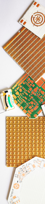
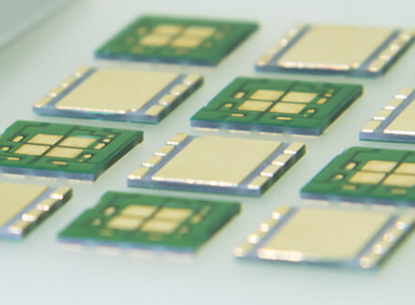
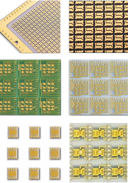
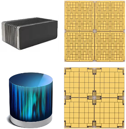
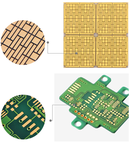
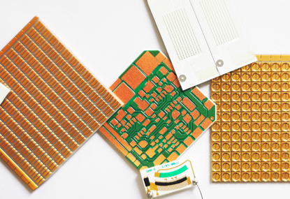
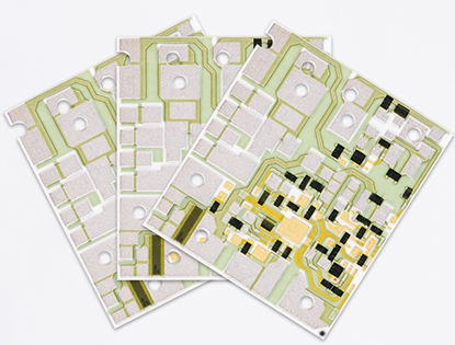
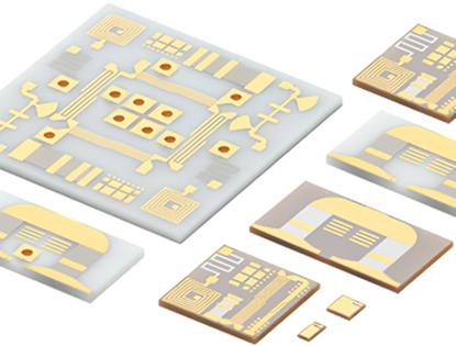
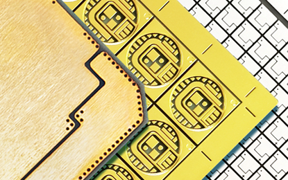
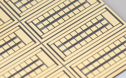
Ceramic PCB
Ceramic PCBs, also known as Ceramic Substrate PCBs, are high-performance printed circuit boards that utilize ceramic materials (aluminum oxide, aluminum nitride, and beryllium oxide) as substrates, offering excellent thermal conductivity, mechanical strength, and insulation properties, with manufacturing processes involving thin-film metallization or thick-film metallization techniques to apply conductive materials to the substrates, followed by etching or high-temperature sintering to create highly reliable circuits, making them widely used in electronic systems requiring high power, high frequency, and high thermal conductivity, such as LED drivers, lasers, communication, automotive electronics, aerospace, and medical fields. Ceramic PCBs provide exceptional functionality in high-performance electronic systems. One of their key features is their outstanding thermal management capabilities. The high thermal conductivity of the ceramic substrates allows heat to be quickly dissipated, making them particularly suitable for power electronics, high-frequency applications, and systems that generate significant heat during operation. Additionally, Ceramic PCBs offer excellent electrical insulation, ensuring that circuits remain stable and free from interference. Ceramic PCBs (Ceramic Printed Circuit Boards) find applications across a wide range of industries due to their superior performance and durability. In the telecommunications industry, Ceramic PCBs are used in high-frequency RF circuits, antennas, and microwave devices, where thermal management and signal integrity are paramount. In power electronics, they are used in power modules, LED lighting, and automotive electronics, where high power and heat loads are common. Furthermore, Ceramic PCBs are extensively used in aerospace and military applications, where reliability and resistance to extreme conditions are crucial. Main Features of Ceramic PCB : |
 |
|
 |
1, High thermal conductivity: Ceramic PCBs exhibit excellent thermal conductivity, facilitating efficient heat dissipation and cooling. 2, Low coefficient of thermal expansion (CTE): Ceramic PCBs typically have a low CTE, which helps minimize the risk of thermal stress and failure, particularly in environments with fluctuating temperatures. 3, Electrical insulation: Ceramic materials used in PCBs offer high electrical insulation properties, making them suitable for applications requiring strong insulation characteristics. 4, Mechanical stability: Ceramic PCBs provide robust mechanical stability, ensuring durability and reliability in various operating conditions. |
|
|
5, Compatibility with leadless ceramic chip carriers: Ceramic PCBs often share compatible CTE with leadless ceramic chip carriers, contributing to improved thermal performance and reliability in electronic assemblies. 6, Compatibility with high-temperature applications: Ceramic PCBs can withstand high operating temperatures, making them suitable for use in demanding environments such as aerospace, automotive, and power electronics. These properties collectively make ceramic PCBs well-suited for applications that demand superior thermal management, high reliability, and insulation in challenging operating conditions. |
||
Material Properties of Ceramic PCB : |
|
1, Base Materials: The base materials used in ceramic PCBs include 96% or 98% aluminum oxide (Al2O3), aluminum nitride (ALN), and beryllium oxide (BeO). 2, Conductor Materials: Conductor materials can include plated copper, silver palladium (AgPd), gold palladium (AuPd), and Direct Copper Bonded (DCB) technology. |
|
 |
3, Application Temperature Range: Ceramic PCBs have an application temperature range of -55°C to 850°C. 4, Thermal Conductivity Values: Thermal conductivity values range from 24W/m-K to 28W/m-K for Al2O3, 150W/m-K to 240W/m-K for ALN, and 220W/m-K to 250W/m-K for BeO. 5, Maximum Compression Strength: Ceramic PCBs typically exhibit a compression strength exceeding 7,000 N/cm2. 6, Breakdown Voltage: The breakdown voltage ranges from 15 KV/mm to 28 KV/mm for thicknesses of 0.25mm, 0.63mm, and 1.0mm respectively. 7, Thermal Expansion Coefficient: The thermal expansion coefficient is approximately 7.4 ppm/K (between 50°C and 200°C). 8, High-Temperature Operation: Ceramic PCBs can safely operate at temperatures up to 350 degrees Celsius. |
|
9, Cost-Efficiency: Ceramic PCBs offer lower system costs by reducing testing, insertion, and assembly requirements. 10, Hermetic Packaging and Low Water Absorption: Ceramic PCBs enable hermetic packaging and feature 0% water absorption, enhancing their reliability and performance in various applications. |
|
Advantages of Ceramic Substrate PCB : |
|
1, Excellent Electrical Insulation: 2, High Operating Temperatures: |
|
 |
3, Adaptability: 4, Durability: 5, Versatility: 6, Stability: |
|
7, Miniaturization and High Density: 8, Corrosion Resistance: 9, Environmental Friendliness: |
|
Optional Substrates of Ceramic PCB : |
Substrates : |
Alumina (Al2O3) |
Aluminum Nitride (AlN) |
Beryllium Oxide (BeO) |
Zirconium Dioxide (ZrO2) |
Max Application Temperature : |
662 - 1832 |
1832 |
2300 |
2432 |
Max Power Density (W/in²): |
75 |
1010 |
250 |
300 |
Max Ramp Up Speed (°F/sec): |
122 |
572 |
400 |
350 |
Thermal Conductivity (W/mK): |
20-35 |
180-220 |
200-300 |
2.0-5.0 |
Density (g/cm³): |
3.75 |
3.26 |
2.8 |
5.9 |
Dielectric Loss: |
0.0001 - 0.001 |
0.0001 - 0.0005 |
0.0001 - 0.0002 |
0.0005 - 0.001 |
Dielectric Constant: |
9.4 - 10.2 |
8.5 - 9.0 |
6.0 - 7.0 |
25 - 30 |
CTE, ppm/ºC: |
6.0 - 8.0 |
4.0 - 5.0 |
7.0 - 9.0 |
10.0 - 11.0 |
Substrate Thickness (mm): |
0.25 - 2.0 |
0.25 - 2.0 |
0.25 - 2.0 |
0.25 - 2.0 |
Typical Max. Dimension (inch): |
6 x 12 |
5 x 11 |
6 x 6 |
4 x 4 |
Theoretical Total Wattage (W): |
5400 |
55000 |
15000 |
20000 |
Typical Applications of Ceramic Printed Circuit Board : |
|
1, Aerospace and Defense: The aerospace and defense sectors utilize Ceramic Printed Circuit Boards in various applications, including radar systems, avionics, missile guidance systems, satellite communications, and electronic warfare systems. The exceptional mechanical strength, temperature resistance, and high-frequency capabilities of ceramics make them suitable for demanding environments. 2, LED Lighting: Ceramic Printed Circuit Boards find significant application in LED lighting products. The high thermal conductivity of ceramics enables effective heat dissipation, which is crucial for maintaining LED performance and extending their lifespan. Additionally, the excellent electrical insulation properties of ceramics ensure reliable electrical connections for LEDs. |
|
 |
3, Medical Devices: Ceramic PCBs are utilized in medical devices like implantable devices, diagnostic equipment, surgical instruments, and laboratory analysis systems. The biocompatibility of ceramics, along with their ability to withstand sterilization processes and provide high-density interconnects, makes them suitable for medical applications. 4, Power Electronics: Ceramic PCBs are extensively used in power electronic devices such as inverters, converters, motor drives, and power modules. The excellent thermal conductivity of ceramics helps in dissipating heat generated during high-power operations, ensuring efficient performance and reliability. 5, Telecommunications: Ceramic PCBs are found in telecommunications equipment such as base stations, antennas, routers, and high-speed data transmission devices. The low dielectric loss and excellent signal integrity of ceramics enable the efficient transmission of high-frequency signals without degradation. 6, Industrial Equipment: Ceramic PCBs are employed in various industrial equipment, including power supplies, robotics, control systems, and monitoring devices. The high thermal conductivity and reliability of ceramics contribute to the proper functioning of these systems in harsh industrial environments. |
|
7, Automotive Electronics: With the increasing complexity of automotive electronics, Ceramic Printed Circuit Boards are employed in advanced driver-assistance systems (ADAS), engine control units (ECUs), lighting systems, and power management modules. The superior thermal and electrical properties of ceramics ensure stable performance and longevity even in high-temperature conditions. Ceramic Printed Circuit Boards are extensively used in a wide range of applications where high-performance, reliability, thermal management, and electrical insulation are crucial. Their unique properties make them well-suited for demanding industries such as power electronics, automotive, aerospace, medical, telecommunications, and industrial sectors. |
|
Differences Between FR4 PCB and Ceramic PCB : |
1, Material Characteristics: |
|
 |
2, Manufacturing Processes: 3, Thermal Performance: 4, Moisture Absorption: |
5, High-Frequency Applications: |
|
 |
6, Material Costs: 7, Product Applications: |
While FR4 PCBs are cost-effective and suitable for general-purpose applications, Ceramic PCBs offer superior thermal performance, high-frequency capabilities, and enhanced reliability, making them ideal for demanding applications in industries where heat dissipation and high-frequency signal integrity are critical. |
|
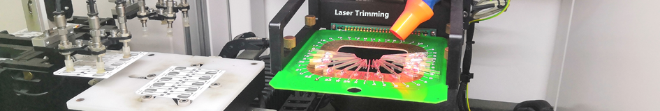
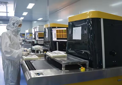
Manufacturing Challenges of Ceramic Printed Circuit Board : |
Manufacturing Ceramic Printed Circuit Boards presents several unique challenges compared to traditional FR4 PCBs due to the properties of ceramic materials and the specialized processes involved. Some of the key manufacturing challenges encountered with ceramic PCBs include: 1, Material Handling: Ceramic materials, such as alumina or aluminum nitride, are brittle and can be prone to chipping or cracking during handling and processing. Special care must be taken to prevent damage to the ceramic substrates throughout the manufacturing process. |
|
 |
2, Machining and Processing: Ceramics are significantly harder and more abrasive than traditional PCB materials like FR4. Machining processes such as drilling, routing, and milling ceramic substrates require special tools and techniques to achieve precise features without causing micro-cracks or delamination. 3, Metallization and Adhesion: Achieving reliable adhesion between the ceramic substrate and metal traces is crucial for the performance of ceramic PCBs. Metallization processes, such as screen printing conductive pastes or sputtering metal layers, must be carefully controlled to ensure good adhesion and prevent delamination. 4, Via Formation: Creating vias in ceramic PCBs can be challenging due to the hardness of the material. Laser drilling or punching techniques are commonly used to form vias, but these processes require precise control to avoid micro-cracks, debris accumulation, or thermal damage to the substrate. |
|
5, Surface Finish and Coating: Ceramic PCBs may require specialized surface finishes or coatings to protect the substrate from environmental factors, improve solderability, or enhance electrical properties. Selecting compatible surface finishes and applying them uniformly on ceramic surfaces can be a challenge during manufacturing. 6, Dimensional Stability: Ceramics exhibit low thermal expansion coefficients, which can lead to dimensional stability challenges during manufacturing processes involving high-temperature exposure, such as sintering or firing. Controlling shrinkage rates and maintaining tight tolerances on feature sizes are critical for ensuring dimensional stability in ceramic PCB production. |
|
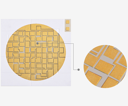
Thin Film Metallization VS Thick Film Metallization Technology : |
In the process of metallization on Ceramic PCB, thick film metallization technology and thin film metallization technology are two commonly used PCB processes. They differ significantly in terms of production processes, technical characteristics, advantages, and disadvantages. |
|
 |
Production Process: Technical Characteristics: ● Simpler process: Compared to thin film technology, the thick film process is simpler, making it more suitable for large-scale production. ● Lower cost: Because the process is relatively simple and the raw materials are inexpensive, it is suitable for cost-sensitive applications. |
Advantages: ● Stronger adaptability: Thick film metallization requires lower-quality substrates, allowing for less precise ceramic surfaces, thus simplifying production. ● Lower cost: Compared to thin film processes, thick film technology typically has lower production costs. Disadvantages: ● Poorer thermal stability: Thick film metallization may experience thermal expansion mismatches at high temperatures, affecting system stability. ● Higher surface roughness: Due to the thicker metal layer, the surface is rougher, which may affect performance in high-precision applications. |
|
 |
Production Process: Technical Characteristics: ● High precision: Thin film technology allows for the creation of very precise circuit patterns, making it suitable for applications requiring high precision and density. ● Material flexibility: A variety of materials (such as gold, aluminum, copper, etc.) can be used for deposition, meeting the needs of different applications. |
Advantages: ● Good thermal stability: Thin film metallization tends to offer better thermal stability, making it suitable for environments with high thermal demands. ● Smooth surface: The metal layer is uniformly thin and the surface is smooth, which is beneficial for high-frequency and high-speed applications. Disadvantages: ● Lower current carrying capacity: Since the metal layer is thin, it is not suitable for high-current applications, which may limit its use in power-intensive applications. ● Higher substrate requirements: Thin film processes usually require a high-quality substrate with a smooth and clean surface to achieve precise metal deposition. |
|
|
● Thick Film Metallization Technology is more suitable for high-power and high-current applications, offering lower production costs and stronger adaptability, but it has limitations in terms of precision and thermal stability. ● Thin Film Metallization Technology excels in high precision, high-density, high-frequency, and thermal stability, making it ideal for applications with demanding performance requirements, but it is more expensive and less suited for high-current carrying applications. Each technology has its own advantages, and the choice of which process to use typically depends on the specific application needs and the balance between performance requirements and production costs. |
|
Sintering Types of Thick Film Substrates Used For Ceramic PCB : |
Thick Film Substrates are ceramic materials commonly used in Electronic Packaging and Ceramic PCB. There are two main types based on sintering temperature: High-Temperature Co-fired Ceramic (HTCC) and Low-Temperature Co-fired Ceramic (LTCC). These two technologies differ significantly in terms of material composition, sintering temperature, and applicable ranges, making them suitable for different electronic applications. |
|
 |
1. High-Temperature Co-fired Ceramic (HTCC) Applications: |
Characteristics: ● Higher material strength: Due to the use of high-temperature ceramics, HTCC materials have greater structural strength, allowing them to withstand significant mechanical stress. ● Larger substrate sizes: HTCC is suitable for larger circuit substrates and provides good electrical isolation performance. ● Complex processing: Due to the high sintering temperature, the process requires precise control, making it more complex and expensive compared to other technologies. |
|
 |
2. Low-Temperature Co-fired Ceramic (LTCC) Applications: |
Characteristics: ● High-density integration: LTCC allows for the integration of high-density circuits and multi-layer designs. Multiple circuit layers can be incorporated into a single substrate, making it ideal for miniaturized, complex electronics. ● Excellent electrical properties: LTCC provides outstanding electrical performance, especially for high-frequency applications, with good electrical insulation that helps reduce signal loss. ● Miniaturization suitability: LTCC substrates support multi-layer circuits and small-size designs, ideal for highly integrated, miniaturized devices. ● Lower mechanical strength: Compared to HTCC, LTCC has somewhat lower mechanical strength and may not be suitable for applications requiring large mechanical stress. High-Temperature Co-fired Ceramic (HTCC) is more suitable for high-temperature environments, applications requiring higher mechanical strength, and larger substrates, such as high-frequency circuits and power electronics. Low-Temperature Co-fired Ceramic (LTCC) is ideal for small-size, high-density, and multi-layer circuit designs, particularly in applications such as high-frequency communications, sensors, and micro-packaging. Both technologies have their strengths and are chosen based on specific application needs, including operating conditions, electrical performance, and design complexity. |
|
Design Guidelines of Ceramic PCB : |
We compiled a Ceramic PCB-Design Guidelines as attached for you to download, It is to better support our customers' needs in designing and applying Ceramic PCBs, This guide covers detailed information on product solutions, engineering design specifications, material properties, available manufacturing processes, and more. We hope that this guide will assist customers in standardizing their design process while ensuring the manufacturability of the design data, ultimately improving product reliability and production efficiency. Customers are encouraged to refer to the guide when designing Ceramic PCBs to ensure adherence to best practices. |
Optional Processes of Ceramic PCB : |
Metalization Types : |
Thick Film Substrates (Screen-Printed) |
Thin Film Substrates (Photo-Imaged) |
|||
Process Types : |
TFM Capabilities |
HTCC / LTCC Capabilities |
DBC Capabilities |
DPC Capabilities |
AMB Capabilities |
Layer Counts : |
1, 2, 3, 4, 5, 6 Layers |
1, 2, 4, 6, 8, 10, 12 Layers |
1, 2 Layers |
1, 2 Layers |
1, 2 Layers |
Max Board Dimension : |
200*230mm |
200*200mm |
138*178mm |
138*190mm |
114*114mm |
Min Board Thickness : |
0.25mm |
0.25mm |
0.30mm~0.40mm |
0.25mm |
0.25mm |
Max Board Thickness : |
2.2mm |
2.0mm |
1L: 1.6mm; 2L 2.0mm |
2.0mm |
1.8mm |
Conductor Thickness : |
10um - 20um |
5um - 1500um |
1oz - 9oz |
1um - 1000um |
1oz- 22oz |
Min Line Width/Space : |
8/8mil (0.20/0.20mm) |
6/6mil (0.15/0.15mm) |
10/10mil (0.25/0.25mm) |
6/6mil (0.15/0.15mm) |
12/12mil (0.30/0.30mm) |
Substrates Types : |
AI203, ALN, BeO, ZrO2 |
AI203, ALN, BeO, ZrO2 |
Al2O3, AlN, ZrO2, PbO, SiO2, ZTA, Si3N4, SiC, Sapphire, Polycrystalline Silicon, Piezoelectric Ceramics |
Al2O3, AlN, ZrO2, PbO, SiO2, ZTA, Si3N4, SiC, Sapphire, Polycrystalline Silicon, Piezoelectric Ceramics |
AI203, ALN, BeO, ZrO2, Si3N4 |
Min Hole Diameter : |
4mil (0.15mm) |
4mil (0.15mm) |
4mil (0.1mm) |
4mil (0.1mm) |
4mil (0.1mm) |
Outline Tolerance : |
Laser: +/-0.05mm; Die Punch: +/-0.10mm |
Laser: +/-0.05mm; Die Punch: +/-0.10mm |
Laser: +/-0.05mm; Die Punch: +/-0.10mm |
Laser: +/-0.05mm; Die Punch: +/-0.10mm |
Laser: +/-0.05mm; Die Punch: +/-0.10mm |
Substrate Thickness : |
0.25, 0.38, 0.50, 0.635, 0.80,1.0, 1.25, 1.5, 2.0mm, Customizable |
0.25, 0.38, 0.50, 0.635, 0.80,1.0, 1.25, 1.5, 2.0mm, Customizable |
0.25, 0.38, 0.50, 0.635, 0.80,1.0, 1.25, 1.5, 2.0mm, Customizable |
0.25, 0.38, 0.50, 0.635, 0.80,1.0, 1.25, 1.5, 2.0mm, Customizable |
0.25, 0.38, 0.50, 0.635, 0.80,1.0, 1.25, 1.5, 2.0mm, Customizable |
Thickness Tolerance : |
0.25-0.38: +/-0.03mm; 0.50-2.00: +/-0.05mm |
0.25-0.38: +/-0.03mm; 0.50-2.00: +/-0.05mm |
0.25-0.38: +/-0.03mm; 0.50-2.00: +/-0.05mm |
0.25-0.38: +/-0.03mm; 0.50-2.00: +/-0.05mm |
0.25-0.38: +/-0.03mm; 0.50-2.00: +/-0.05mm |
Surface Treatment : |
Ag, Au, AgPd, AuPd |
Ag, Au, AgPd, AuPd, Mn/Ni |
OSP/Ni Plating, ENIG |
OSP/ENIG/ENEPIG |
OSP/ENIG/ENEPIG |
Min Solder PAD Dia : |
10mil (0.25mm) |
10mil (0.25mm) |
8mil (0.20mm) |
6mil (0.15mm) |
8mil (0.20mm) |