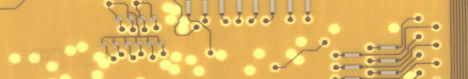
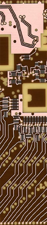
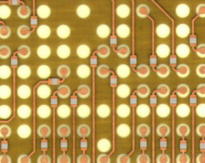
Thin Film Embedded Resistor PCB
Thin Film Embedded Resistor PCBs are high-precision electronic circuits that directly integrate thin film resistors into the printed circuit board's internal layers, with the core process involving the deposition or lamination of thin film resistive materials onto the PCB's inner core, followed by precise techniques such as pattern transfer, etching, and laser trimming to complete the resistor layout, after which additional outer layers are added to form a high-density circuit system that significantly reduces the need for discrete resistive components traditionally required on the PCBs, optimizing the overall circuit design. Thin Film Embedded Resistor PCBs have the key feature of achieving higher functional integration in limited space. The design of these PCBs embeds resistive components, which would otherwise occupy surface space, within the internal layers of the PCB, freeing up more surface area to accommodate additional active components. As thin film resistors offer higher stability, precision, and temperature performance, this embedded design also improves the overall reliability of the device. Thin Film Embedded Resistor PCBs are widely used in electronic devices that require high performance and miniaturization. They are especially valuable in industries such as consumer electronics, communication equipment, automotive electronics, and medical instruments. In these fields, miniaturization and multifunctionality are central design requirements, and embedded thin film resistor PCBs effectively address space limitations while improving the overall functionality and performance of the circuits. Moreover, this technology makes the design of multi-layer PCBs more flexible, enabling better handling of complex electrical connections. Key Features of Thin Film Embedded Resistor PCB : |
 |
|
 |
1, Space Efficiency: 2, High Integration Capability: |
|
3, Enhanced Signal Integrity: 4, Improved Thermal Management: 5, Customizable Resistance Values: 6, Reliability and Stability: 7, Design Flexibility: |
||
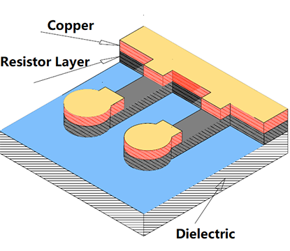
Resistive Foil Materials of Thin Film Embedded Resistor PCB : |
Resistive Foil Materials used in thin film embedded resistor PCBs plays a crucial role in achieving precise resistance values and ensuring reliable performance. Here are some key aspects of resistive foil materials in these PCBs: 1, Thin Film Deposition: 2, Low Temperature Coefficient of Resistance (TCR): |
|
 |
3, High Resistivity: 4, Excellent Linearity: 5, Stability and Reliability: |
6, Compatibility with Manufacturing Processes: 7, Material Compatibility: The resistive foil material in Thin Film Embedded Resistor PCBs are crucial for achieving precise resistance values, stability, reliability, and compatibility with manufacturing processes. These materials are carefully selected for their low TCR, high resistivity, excellent linearity, stability, and compatibility with other PCB materials, enabling the creation of high-performance embedded resistor PCBs for a wide range of applications. |
|
Calculating Resistor Value of Thin Film Embedded Resistor PCB : |
Calculating the resistor value of a thin film embedded resistor PCB involves understanding the dimensions and properties of the resistive foil material deposited on the PCB substrate. Here is a general guide on how to calculate the resistor value: 1, Determine the Dimensions: 2, Calculate the Resistivity: |
|
 |
3, Calculate the Resistance Value: |
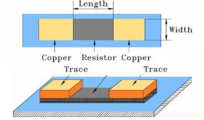
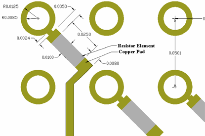
To be simple, All resistor materials are provided with resistance values expressed in ohms per square as : R = pL/A, R is resistance in ohms, p is the resistivity of the material, L is the length and A is the cross sectional area (i.e., thickness times width). When thickness is held constant then R is the same for any square area, hence the expression ohms/square. Resistance then can be varied by varying the aspect ratio of the area (L/W). 4, Adjust for Accuracy: 5, Consider Temperature Coefficient: By following these steps and considering the dimensions, resistivity, and temperature coefficient of the resistive foil material, engineers can accurately calculate the resistor value of a thin film embedded resistor PCB. Fine-tuning the resistance value and ensuring consistency across production batches will result in reliable and high-performance embedded resistor circuits for various electronic applications. |
|
Advantages of Thin Film Embedded Resistor PCB : |
|
1, Improved signal integrity: When resistors are embedded within the PCB, the signal traces can be routed more closely to the resistors, reducing the length of the traces and minimizing parasitic effects like capacitance and inductance. This leads to improved signal integrity, reduced electromagnetic interference (EMI), and better performance of high-speed digital circuits. |
|
 |
2, Enhanced reliability: Thin film embedded resistors are protected within the PCB layers, providing better resistance to environmental factors such as moisture, dust, and physical damage. This improves the overall reliability and durability of the circuit, making it suitable for various demanding applications and operating conditions. 3, Thermal management: Thin Film Embedded Resistor PCBs can have improved thermal dissipation compared to surface-mounted resistors. The close proximity of the resistor to the PCB substrate allows for efficient heat transfer, reducing the risk of overheating and enhancing overall thermal management of the circuit. 4, Reduced manufacturing steps: In traditional PCB assembly, surface-mounted resistors need to be separately placed and soldered onto the PCB. With thin film embedded resistors, there is no need for these additional assembly steps, simplifying the manufacturing process and reducing production costs. |
5, Space-saving: Thin Film Embedded Resistor PCBs eliminate the need for separate surface-mounted resistors, saving valuable space on the PCB. By integrating resistors directly into the PCB layers, it allows for more compact and dense circuit designs. This is particularly beneficial in applications where miniaturization and space constraints are important. |
|
 |
6, Precise resistor characteristics: Thin film technology allows for accurate control of resistor values, tolerance, and temperature coefficients. This ensures consistent and reliable performance of the embedded resistors, meeting the required specifications and tolerances of the circuit design. 7, Design flexibility: Thin Film Embedded Resistor PCBs offer design flexibility as they can be customized to meet specific requirements. The resistance values, power ratings, and distribution of resistors within the PCB layers can be tailored according to the circuit design, allowing for optimized performance and functionality. |
Applications of Thin Film Embedded Resistor PCB : |
1, Aerospace and Defense: Thin Film Embedded Resistor PCBs find application in aerospace and defense systems where space-saving designs and high reliability are essential. These PCBs are used in avionics, radar systems, communication equipment, and missile guidance systems, where stringent performance requirements and resistance to harsh environmental conditions are critical. 2, Medical Devices: In the medical field, Thin Film Embedded Resistor PCBs are employed in various devices such as patient monitoring equipment, diagnostic instruments, imaging systems, and implantable medical devices. Their small form factor and high precision make them suitable for compact and sensitive medical electronics applications. |
|
 |
3, Telecommunications: Telecommunication infrastructure and networking equipment utilize Thin Film Embedded Resistor PCBs for their high integration capability and signal integrity benefits. These PCBs are incorporated into base stations, network switches, routers, and optical communication systems to ensure reliable signal processing and data transmission. 4, Automotive Electronics: Thin Film Embedded Resistor PCBs are integrated into automotive electronics for applications such as engine control units (ECUs), advanced driver-assistance systems (ADAS), infotainment systems, and powertrain control modules. Their space efficiency and resistance to temperature variations make them well-suited for the demanding automotive environment. 5, Industrial Automation: In industrial automation and control systems, Thin Film Embedded Resistor PCBs are utilized in programmable logic controllers (PLCs), motor drives, robotics, and process control equipment. The high reliability and precise resistance values of these PCBs contribute to the stability and accuracy of industrial automation systems. |
6, Consumer Electronics: Thin Film Embedded Resistor PCBs are used in consumer electronics products such as smartphones, tablets, wearables, and IoT devices. Their compact design and high-performance characteristics enable the development of smaller, lightweight, and power-efficient electronic gadgets. 7, Instrumentation and Measurement Equipment: Precision measurement instruments, test and measurement equipment, and scientific instrumentation often incorporate Thin Film Embedded Resistor PCBs for accurate signal processing, data acquisition, and calibration purposes. Their stability, linearity, and customizable resistance values make them suitable for high-precision applications. |
|
Etching Sequence of Thin Film Embedded Resistor PCB : |
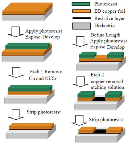 |
1, Materials : 2, Photoresist Application : 3, Exposure : 4, Develop : 5, Etchting Process : 6, Resist Stripping : |
Resistive Foil Specifications of Thin Film Embedded Resistor PCB : |
Resistive materials |
NiCr |
NCAS |
CrSiO |
Sheet resistance (Ω/sq) |
25, 50, 100 |
25, 50, 100, 250 |
1000 |
Sheet resistivity tolerance (%) |
±5 |
±5 |
±5 |
Temperature coefficient of resistance (ppm/°C) |
<110 |
-20 |
300 |
Base copper foil thickness (microns) |
18, 35 |
18, 35 |
18, 35 |
Width maximum mm (inches) |
1295 (51) |
1295 (51) |
1295 (51) |
Maximum recommended power dissipation at 40° C (watts/sq in) |
50 Ω /sq: 200 |
50 Ω /sq: 200 |
1000 Ω/sq: 250 |
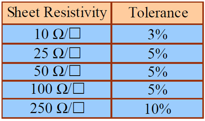
Multiple Sheet Resistivities of Thin Film Embedded Resistor PCB : |
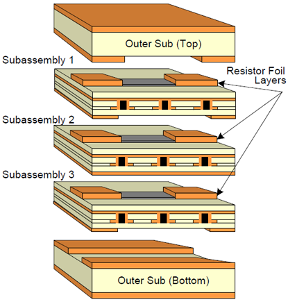 |
1, Embedded resistor layers in a multilayer PCB can be initiated by replacing standard copper foil with a thin film resistor foil on one side of the cores. The specific dielectric material for the cores can be specified in the design or chosen by the PCB fabricator to meet the electrical requirements of the final product. The thin film resistor foil exhibits good peel strength and sheet resistivity values, complementing many commercially available high Tg value, lead-free systems. 2, The inner layers of the subassemblies follow the standard procedure of lamination for a single-layer multilayer PCB. As the resistor layer will serve as the outermost layer of the subassembly, the lay-up process begins with the resistor foil, either free-standing or supported. The prepreg is then applied onto the exposed resistor side of the foil. Care must be taken to prevent the prepreg from sliding over the resistor surface to avoid damaging it. 3, Once the subassemblies are laminated together, the resistor elements become enclosed. Thin Film Embedded Resistor PCB can then undergo the standard sequence of processes including drilling, plating, imaging, etching, surface finishing, soldermask application, routing, and electrical testing. 4, Designing and manufacturing PCBs with embedded resistors, especially with multiple sheet resistivities and layers of buried resistors, can pose challenges. These processes are further complicated by advanced PCB technologies like HDI that are often integrated with embedded passives. |
Design Considerations for Thin Film Embedded Resistor PCB : |
When designing a Thin Film Embedded Resistor PCB, several key considerations should be taken into account to ensure optimal performance and functionality. Some important design considerations include: 1, Resistor Material Selection: Choose the appropriate resistor material based on the desired resistance value, temperature coefficient of resistance (TCR), stability, and reliability requirements. 2, Resistor Layout and Dimension: Optimize the layout and dimensions of the resistors to achieve the required resistance values while minimizing space usage and ensuring proper electrical performance. |
|
 |
3, Embedding Technique: Select the most suitable embedding technique (such as laser trimming, laser direct imaging, or screen printing) based on the design requirements and manufacturing capabilities. 4, Integration with Circuitry: Ensure proper integration of the resistors with the rest of the circuitry to achieve the desired electrical characteristics and signal integrity. 5, Temperature Coefficient Considerations: Take into account the temperature coefficient of resistance (TCR) of the resistors and design for stable performance over the expected operating temperature range. 6, Power Dissipation: Consider the power dissipation requirements of the resistors and ensure that the design can handle the anticipated power levels without overheating. |
7, Signal Integrity and Crosstalk: Minimize signal interference and crosstalk by carefully routing traces and placing components to maintain signal integrity throughout the PCB. 8, Reliability and Durability: Design the PCB to withstand environmental factors, mechanical stress, and other external influences to ensure long-term reliability and durability. 9, Testing and Verification: Plan for testing and verification of the embedded resistors during the design phase to ensure they meet the specified performance criteria and quality standards. By addressing these design considerations effectively, you can optimize the performance, reliability, and manufacturability of thin film embedded resistor PCBs for a wide range of applications. |
|