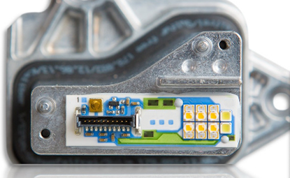
Hybrid Microcircuits
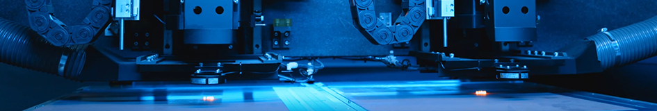
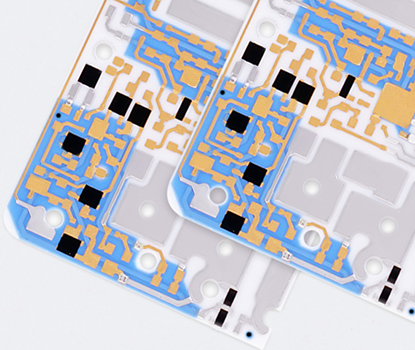
Hybrid Microcircuits, also known as Thick Film Microcircuits, are customizable electronic circuits manufactured using thick-film technology that integrate discrete components (such as diodes, transistors, or monolithic ICs) and passive components (such as inductors, resistors, capacitors, and transformers) onto a single ceramic substrate, making them highly favored for use in harsh environments like aerospace, military, automotive, telecommunications, industrial control, and medical fields due to their compactness, high durability, and reliability. Hybrid Microcircuits serve as components on PCBs in the same way as integrated circuits (ICs) do. The difference between the two types of devices is in how they are constructed and manufactured. These small custom packages result in higher performance modules than may be available through the application of typical commercially available components. In military, automotive, and space applications, numerous integrated circuits, transistors, and diodes, in their die form, would be placed on either a hybrid microcircuit. Either gold or aluminum wire would be bonded from the pads of the ICs, transistors, or diodes to the hybrid microcircuits. Thick Film Microcircuits are a type of microcircuit that use a combination of screen printing and firing techniques to print conductive, resistive, and dielectric materials on a ceramic substrate. The process involves printing successive layers of thick film pastes onto the substrate to form individual components such as resistors, capacitors, and conductive traces. These layers are then fired in a high-temperature furnace to create a solid, permanent structure. Main Features of Hybrid Microcircuits : |
 |
|
 |
1, Integration: Thick film microcircuits can integrate multiple discrete components into a single package, such as resistors, capacitors, and inductors, which can result in reduced size and weight of the overall system. 2, Durability: Hybrid Microcircuits are highly durable and can withstand extreme temperatures, humidity, and mechanical stresses, making them suitable for use in harsh environments. 3, High precision: Thick film technology allows for precise control over the dimensions of each component, resulting in highly accurate and stable circuit elements. 4, Cost-effective: Thick film microcircuits are typically more cost-effective than other microcircuit technologies because they do not require expensive equipment or cleanroom environments for production. |
|
5, Customization: Hybrid Microcircuits allows engineers to customize circuits based on specific requirements by adding or removing components or adjusting parameters such as resistance or capacitance. 6, Higher Versatility: Thick film interconnecting technology offers higher versatility over thin film technology, such as choice of resistor value to be utilized for integrating in the hybrid microcircuits and use of planar resistors among others. And insulating dielectrics developed though screen printing which are utilized for multilayer thick film technique of hybrid microcircuits manufacturing,This technique of usage of insulating dielectrics ensures that the in-between layer connections are made in the required places only, Modern technologies such as low temperature co-fired ceramic (LTCC) allows for development of partial three dimensional hybrid microcircuits. Please refer to Thick Film Technology for more informations. |
||
Market Penetration of Hybrid Microcircuits : |
The market penetration of Hybrid Microcircuits has been significant, particularly in industries that require high-performance and reliable electronic systems. Here are a few factors contributing to their market penetration: 1, Automotive: Hybrid microcircuits are integrated into automotive electronics for functions such as engine control units (ECUs), safety systems, infotainment systems, driver assistance systems, and more. Their ability to handle high power and withstand temperature variations makes them ideal for automotive applications. |
|
 |
2, Telecommunications: With the growing demand for faster and more efficient communication systems, hybrid microcircuits play a crucial role in telecommunications infrastructure. They are employed in base stations, optical networking devices, network switches, routers, and other telecommunications equipment. 3, Energy Systems: Thick Film Microcircuits are used in various energy systems, including renewable energy generation, power distribution, and smart grid management. They contribute to the efficiency, monitoring, and control of these systems. 4, Industrial Automation: Industrial automation relies on sophisticated control systems, and hybrid microcircuits enable precise control and data processing in these applications. They are employed in programmable logic controllers (PLCs), motor drives, robotics, sensors, and monitoring systems. 5, Medical Devices: Hybrid microcircuits find extensive usage in the medical industry for various applications. They are utilized in monitoring and diagnostic equipment, implantable devices, surgical instruments, imaging systems, and other medical electronics that demand high precision, reliability, and compactness. |
6, Aerospace and Defense: Thick Film Microcircuits are widely used in aerospace and defense applications due to their ability to withstand challenging environmental conditions, such as extreme temperatures, vibrations, and shocks. They are employed in aircraft avionics, radar systems, satellite communications, missile guidance systems, and more. The market penetration of thick film microcircuits continues to expand as industries increasingly demand high-performance, reliable, and compact electronic solutions. The continuous advancements in hybrid microcircuit technology and their adaptability to diverse applications contribute to their growing popularity and market penetration. |
|
Advantages of Hybrid Microcircuits : |
1, High Temperature Applications: When electronics operate at elevated temperatures the materials used can have a substantial impact on performance and life. With its ability to dispel heat, ceramic substrate performs better and can prevent a device from being damaged by high temperatures. Depending on the material used, like Alumina or Aluminum Oxide, Aluminum nitride (AlN), beryllia or beryllium oxide (BeO), silicon carbide, and boron nitride, the values range from 20 to 300 W/(m·K). It is way beyond that of FR-4 printe circuit board, more than 20x higher. 2, Low Coefficient of Thermal Expansion (CTE): Ceramic substrate has solid and outstanding interatomic bonds, so Hybrid Microcircuits can withstand high temperatures and is still firm, stable, and steady even under changing temperatures. 3, Low Failure Rate: Aside from long term reliability, Ceramic Hybrid Microcircuits also exhibit a lower mean time between failure rate when exposed to environmental stresses such as high temperature, mechanical vibration or other harsh conditions. |
|
 |
4, Long Term Reliability: Most commercially packaged semiconductors will have a life span measured in years, while hybrids have a life span measured in decades. 5, Custom Packaging: Ceramic Hybrid Microcircuits, or custom monolithic IC packages, provide flexibility for shape and package style, as well as the option for improved performance. 6, Inorganic: Due to ceramic is the inorganic materials, so ceramic hybrid microcircuits can work and be of use for a longer period of time. Also, the chemical resistance to erosion is impressive. 7, Small Size and Weight: In applications where a high premium is placed on small size and weight, such as aircraft, missiles, Ceramic Hybrid Microcircuits can offer an extremely compact, high performance solution. 8, High Frequency: High frequency can be handled by a ceramic hybrid microcircuit with its dimensional and thermal stability. Industries requiring high-frequency data and electrical signal transmissions. |
9, Multi-Layering: A multi-layer ceramic PCB can do a more complicated task. With the toughness of its material, another layer can be added easily and still keep the other components safe. Ceramic Hybrid Microcircuit is excellent for heavy-duty applications. 10, Excellent Thermal Insulation: Ceramic substrate is incredibly insulating; therefore, heat will be less likely to flow through the substrate, preserving the ceramic hybrid microcircuit's components from getting damaged or harmed. 11, Cost Efficiency: Ceramic Hybrid Microcircuits may not come cheap outright compared to FR-4 circuit board, but with its improved performance and service life, it will surely last longer. With ceramic hybrid microcircuits simple design and reduced fabrication, the overall system cost is still lower than FR4 PCB or metal core PCBs. |
|
Manufacturing Processes of Hybrid Microcircuits : |
Hybrid Microcircuits (HMCs) are electronic devices that combine the advantages of integrated circuits (ICs) and discrete components. The manufacturing parameters of hybrid microcircuits involve various aspects, including the materials used, assembly techniques, and electrical specifications. Here are some key parameters: 1, Substrate: The substrate material used in Hybrid microcircuit is typically ceramic, such as alumina or beryllium oxide (BeO), due to their excellent thermal conductivity and mechanical stability. 2, Thin Film Deposition: Thin films of conductive and insulating materials are deposited on the substrate using techniques like physical vapor deposition (PVD) or chemical vapor deposition (CVD). These films create the interconnects and insulation layers within the circuit. |
|
 |
3, Die Attach: Active components like diodes, transistors, and integrated circuits are die-bonded onto the substrate using epoxy or solder. This step ensures proper mechanical and electrical connection between the die and the substrate. 4, Wire Bonding: Thin wires made of gold, aluminum, or copper are bonded between the individual components and the substrate to establish electrical connections. 5, Thick Film Printing: Thick film printing involves screen-printing conductive pastes onto the substrate to form resistors, capacitors, and other passive components. The printed layers are then fired at high temperatures to achieve the desired properties. 6, Encapsulation: The entire Hybrid microcircuit is encapsulated using a protective material, commonly epoxy or a hermetic seal. This safeguards the circuit from environmental factors like moisture, dust, and mechanical stress. 7, Semiconductor Integration: Active components like transistors, diodes, and integrated circuits are attached to the substrate using wire bonding or flip-chip techniques. These components are sourced from separate semiconductor fabrication. |
8, Encapsulation: The hybrid microcircuit is encapsulated to protect it from environmental factors such as moisture, dust, and mechanical stress. Epoxy or molded plastic is commonly used for encapsulation. 9, Testing: The completed hybrid microcircuits undergo extensive electrical testing to ensure their functionality and performance meet design specifications. This includes checks for continuity, resistance, capacitance, and other parameters. 10, Packaging: The tested and verified hybrid microcircuits are packaged in appropriate casings or containers for easy integration into larger electronic systems. The packaging provides mechanical protection and facilitates connection to external devices. 11, Quality Control: Throughout the production process, strict quality control measures are implemented to ensure consistent and reliable performance of each hybrid microcircuit. This includes inspections, statistical process control, and failure analysis. 12, Final Inspection: Before the hybrid microcircuits are shipped to customers, a final inspection is conducted to verify their overall quality and adherence to specifications. Any defective units are identified and removed from the batch. |
|
Design Guideline of Thick Film Microcircuits : |
Designing Thick Film Microcircuits requires careful consideration of various factors to ensure optimal performance, reliability, and manufacturability. Here are some general design guidelines for hybrid microcircuits: 1, Component Selection: Choose components (both ICs and discrete) that meet the required specifications for the circuit. Consider factors such as voltage range, current ratings, temperature requirements, and signal characteristics. Select components with compatible package styles and sizes to facilitate integration. 2, Substrate Material: Select a suitable substrate material based on the specific application requirements. Common substrate materials include ceramic, glass, or organic materials like FR-4. Consider factors such as thermal conductivity, dielectric properties, and compatibility with the assembly process. |
|
 |
3, Circuit Layout: Plan the layout of the hybrid microcircuit carefully to optimize performance and minimize signal interference. Place components strategically to minimize the length of signal paths, reduce crosstalk, and ensure proper heat dissipation. Follow best practices for trace routing, power distribution, and grounding. 4, Interconnects: Determine the interconnection method based on the circuit complexity and performance requirements. This can include wire bonding, soldering, flip-chip, or conductive adhesive techniques. Ensure proper alignment and spacing of interconnects to avoid short circuits or open connections. 5, Thermal Management: Consider thermal management during the design phase to prevent overheating and ensure long-term reliability. Use heat sinks, thermal vias, or other cooling mechanisms as necessary. Ensure that heat-generating components are adequately spaced and thermally connected to the substrate. 6, Manufacturing Considerations: Design for manufacturability by considering the capabilities and limitations of the manufacturing process. Consult with the manufacturer early in the design phase to understand their requirements and guidelines. |
7, Environmental Considerations: Take into account the operating environment of the hybrid microcircuit. Consider factors such as temperature extremes, humidity, vibration, and shock. Design the circuit to withstand these conditions by selecting appropriate materials, coatings, and protective measures. 8, Testing and Quality Control: Plan for testing and quality control during the design phase. Incorporate test points, probe pads, or other access points to allow for functional and electrical testing at various stages of manufacturing and assembly. It is important to note that these guidelines provide a general overview, and the specific design considerations may vary depending on the application, technology, and manufacturing process being used. Consulting with our experienced design engineers can help you to ensure a successful hybrid microcircuit design. |
|
Why PANDA PCB For Thick Film Microcircuits ? |
PANDA PCB Group is a leading manufacturer of Thick Film Hybrid Circuits with over 20 years of experience in the design and fabrication, and there are several reasons why we are an excellent choice for this technology. ● Panda PCB has many years of experience in the field of thick film hybrid circuits. Our team of engineers possesses extensive knowledge and expertise in designing and manufacturing these circuits, ensuring that our products are of the highest quality. ● Panda PCB is committed to providing high-quality products to their customers. We use only the best materials and follow strict quality control processes to ensure that each thick film hybrid circuit meets or exceeds industry standards. This dedication to quality translates into durable and reliable products that are built to last. |
|
 |
● Panda PCB Group offers customization options to meet the specific needs of their clients. We understand that each application may have unique requirements, and we are willing to work with our customers to develop a custom solution that fits their needs. ● Panda PCB Group is a reputable and reliable provider of thick film hybrid circuits. Our expertise, focus on quality, customization options, advanced manufacturing facilities, and commitment to customer satisfaction make them an excellent choice for anyone in need of thick film hybrid circuits. |
Capabilities of Hybrid Microcircuits : |
1, Optional Processes of Hybrid Microcircuits :
Metalization Types : |
Thick Film Substrates (Screen-Printed) |
Thin Film Substrates (Photo-Imaged) |
|||
Process Types : |
TFM Capabilities |
HTCC / LTCC Capabilities |
DBC Capabilities |
DPC Capabilities |
AMB Capabilities |
Layer Counts : |
1, 2, 3, 4, 5, 6 Layers |
1, 2, 4, 6, 8, 10, 12 Layers |
1, 2 Layers |
1, 2 Layers |
1, 2 Layers |
Max Board Dimension : |
200*230mm |
200*200mm |
138*178mm |
138*190mm |
114*114mm |
Min Board Thickness : |
0.25mm |
0.25mm |
0.30mm~0.40mm |
0.25mm |
0.25mm |
Max Board Thickness : |
2.2mm |
2.0mm |
1L: 1.6mm; 2L 2.0mm |
2.0mm |
1.8mm |
Conductor Thickness : |
10um - 20um |
5um - 1500um |
1oz - 9oz |
1um - 1000um |
1oz- 22oz |
Min Line Width/Space : |
8/8mil (0.20/0.20mm) |
6/6mil (0.15/0.15mm) |
10/10mil (0.25/0.25mm) |
6/6mil (0.15/0.15mm) |
12/12mil (0.30/0.30mm) |
Substrates Types : |
AI203, ALN, BeO, ZrO2 |
AI203, ALN, BeO, ZrO2 |
Al2O3, AlN, ZrO2, PbO, SiO2, ZTA, Si3N4, SiC, Sapphire, Polycrystalline Silicon, Piezoelectric Ceramics |
Al2O3, AlN, ZrO2, PbO, SiO2, ZTA, Si3N4, SiC, Sapphire, Polycrystalline Silicon, Piezoelectric Ceramics |
AI203, ALN, BeO, ZrO2, Si3N4 |
Min Hole Diameter : |
4mil (0.15mm) |
4mil (0.15mm) |
4mil (0.1mm) |
4mil (0.1mm) |
4mil (0.1mm) |
Outline Tolerance : |
Laser: +/-0.05mm; Die Punch: +/-0.10mm |
Laser: +/-0.05mm; Die Punch: +/-0.10mm |
Laser: +/-0.05mm; Die Punch: +/-0.10mm |
Laser: +/-0.05mm; Die Punch: +/-0.10mm |
Laser: +/-0.05mm; Die Punch: +/-0.10mm |
Substrate Thickness : |
0.25, 0.38, 0.50, 0.635, 0.80,1.0, 1.25, 1.5, 2.0mm, Customizable |
0.25, 0.38, 0.50, 0.635, 0.80,1.0, 1.25, 1.5, 2.0mm, Customizable |
0.25, 0.38, 0.50, 0.635, 0.80,1.0, 1.25, 1.5, 2.0mm, Customizable |
0.25, 0.38, 0.50, 0.635, 0.80,1.0, 1.25, 1.5, 2.0mm, Customizable |
0.25, 0.38, 0.50, 0.635, 0.80,1.0, 1.25, 1.5, 2.0mm, Customizable |
Thickness Tolerance : |
0.25-0.38: +/-0.03mm; 0.50-2.00: +/-0.05mm |
0.25-0.38: +/-0.03mm; 0.50-2.00: +/-0.05mm |
0.25-0.38: +/-0.03mm; 0.50-2.00: +/-0.05mm |
0.25-0.38: +/-0.03mm; 0.50-2.00: +/-0.05mm |
0.25-0.38: +/-0.03mm; 0.50-2.00: +/-0.05mm |
Surface Treatment : |
Ag, Au, AgPd, AuPd |
Ag, Au, AgPd, AuPd, Mn/Ni |
OSP/Ni Plating, ENIG |
OSP/ENIG/ENEPIG |
OSP/ENIG/ENEPIG |
Min Solder PAD Dia : |
10mil (0.25mm) |
10mil (0.25mm) |
8mil (0.20mm) |
6mil (0.15mm) |
8mil (0.20mm) |
2, Optional Substrates of Hybrid Microcircuits :
Substrates : |
Alumina (Al2O3) |
Aluminum Nitride (AlN) |
Beryllium Oxide (BeO) |
Zirconium Dioxide (ZrO2) |
Max Application Temperature : |
662 - 1832 |
1832 |
2300 |
2432 |
Max Power Density (W/in²): |
75 |
1010 |
250 |
300 |
Max Ramp Up Speed (°F/sec): |
122 |
572 |
400 |
350 |
Thermal Conductivity (W/mK): |
20-35 |
180-220 |
200-300 |
2.0-5.0 |
Density (g/cm³): |
3.75 |
3.26 |
2.8 |
5.9 |
Dielectric Loss: |
0.0001 - 0.001 |
0.0001 - 0.0005 |
0.0001 - 0.0002 |
0.0005 - 0.001 |
Dielectric Constant: |
9.4 - 10.2 |
8.5 - 9.0 |
6.0 - 7.0 |
25 - 30 |
CTE, ppm/ºC: |
6.0 - 8.0 |
4.0 - 5.0 |
7.0 - 9.0 |
10.0 - 11.0 |
Substrate Thickness (mm): |
0.25 - 2.0 |
0.25 - 2.0 |
0.25 - 2.0 |
0.25 - 2.0 |
Typical Max. Dimension (inch): |
6 x 12 |
5 x 11 |
6 x 6 |
4 x 4 |
Theoretical Total Wattage (W): |
5400 |
55000 |
15000 |
20000 |
3, Conductive Paste of Hybrid Microcircuits :
Paste ( Materials) : |
Conductor Width/Space |
Soldering / Bonding |
Gold : |
8/8mil (0.20/0.20mm) |
Gold is a good conductor material and allows thermo-compression gold wire bonding and eutectic die attachment. It is, of course, costly and has poor solderability. |
Silver : |
8/8mil (0.20/0.20mm) |
Soldering & Silver is lower in cost, and solderable, but is not leach-resistant with tin/lead solders.More seriously, silver atoms migrate under the influence of DC electric fields, both causing short-circuits and reacting with many of the resistor paste formulations. |
Platinum-Silver : |
6/6mil (0.15/0.15mm) |
Soldering & Surface Mount, Palladium and platinum alloyed to the gold and silver produce good conductor pastes,with good adhesion to the substrate, good solderability, and moderately good wire bonding characteristics.. Copper and nickel are examples of materials that have been proposed for paste systems as substitutes for noble metals. |
Palladium-Silver : |
8/8mil (0.20/0.20mm) |
Soldering & Surface Mount ,Solderable, Wire bondable, (good aged adhesion general purpose), Silver-palladium conductor inks are the most commonly used materials, with both price and performance (primarily resistance to solder) increasing with palladium content. |
Platinum-Gold : |
6/6mil (0.15/0.15mm) |
Soldering & Au or Al Wire Bonding, Solderable (excellent aged adhesion with no migration). |
Palladium-Gold : |
8/8mil (0.20/0.20mm) |
Soldering & Au or Al Wire Bonding, Wire bondable. |
4, Resistive Paste of Hybrid Microcircuits :
Performances : |
Common Values/Range |
Description |
Resistance Value : |
1Ω to several MΩ |
The resistance value depends on the type and ratio of carbon black, typically ranging from 1Ω to Mega ohm. |
Resistance Tolerance : |
±1% to ±10% |
High-precision resistors can achieve ±0.1% tolerance used laser trimming process. |
Temperature Coefficient (TCR) : |
±50ppm/°C to ±200ppm/°C |
High-quality resistive paste should have a low TCR, preferably below ±100ppm/°C. |
Stability : |
≤1% |
Resistors must undergo high-temperature aging and humidity tests to ensure stability. |
Sintering Temperature : |
850°C to 950°C |
The sintering temperature for carbon paste depends on material properties, typically in this range. |
Conductivity : |
10⁶ S/m to 10⁸ S/m |
Conductivity depends on the type and ratio of carbon black, affecting resistance precision and stability. |
Surface Smoothness : |
Ra≤ 1 μm |
The surface must be free of cracks, bubbles, and non-uniform layers to ensure good mechanical and electrical properties. |
Insulation Resistance : |
≥10⁹ Ω |
Carbon paste should have good insulation properties to avoid leakage or short circuits. |
Mechanical Strength : |
≥100 MPa |
The resistive layer must have good compressive and bending strength to ensure the reliability of the resistor. |
Volatility : |
Solvent residue ≤ 1% |
High volatility solvents help with even coating and drying, but excessive volatility may affect electrical performance. |
Oxidation Resistance : |
>1000 hours |
High-quality carbon paste should have strong oxidation resistance to extend the service life. |
Humidity Resistance : |
≥1000 hours |
Resistors should be able to withstand high-humidity conditions to ensure long-term stable performance, no significant changes. |
5, Dielectric Paste of Hybrid Microcircuits :
1, High dielectric strength, That can be printed between two conductor layers as a insulating layer for Multilayer-Thick Film Hybrid Microcircuits. |
6, Insulating Paste of Hybrid Microcircuits :
The insulating layer in a hybrid microcircuit serves to electrically isolate various circuit elements from one another and provide mechanical support for the components. The choice of insulating layer material depends on the specific application requirements and manufacturing process used. Common materials used as insulating layers in hybrid microcircuits include: 1, Glass: Overglazes (Glass-Glaze) is another insulating material that can be used in hybrid microcircuits. Glass substrates can be used as a base for thick-film resistors and other passive components, which are then applied using screen printing and firing techniques. Glass has good electrical and thermal properties, but is more brittle than ceramic. 2, Thick-Film Polymer: Polymer-based insulating materials can also be used in hybrid microcircuits. This involves applying a thick-film polymer material to a substrate, followed by curing at high temperatures to produce a hard, durable layer. Polymer insulating materials have the advantage of being flexible and less brittle than ceramics or glass. 3, Organic: Organic insulating materials, such as epoxy or polyimide, can be used in hybrid microcircuits. These materials offer good insulation properties, as well as flexibility and ease of use. Organic materials can be applied using photolithography or screen printing techniques, depending on the application. |