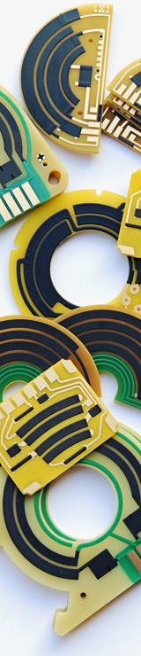
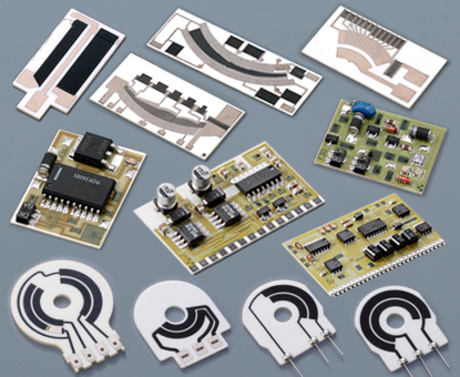
Thick Film Resistor PCB
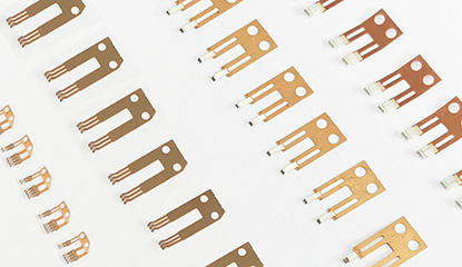
Thick Film Resistor PCBs are efficient, unique circuit boards that integrate resistors, sensors, or heating elements into electronic circuits using thick-film technology, which prints dielectric, conductive, resistive, or insulating materials onto PI, FR4, or ceramic PCBs, followed by curing, sintering, laser trimming, and polishing to create precise, reliable hybrid circuits tailored for various electronic systems. Thick Film Resistor PCBs offer great flexibility in customization, allowing designers to select resistive values and power ratings based on specific needs. The thick-film technology ensures high precision and stability, even in extreme conditions. These PCBs are highly durable, with excellent thermal stability and resistance to humidity and vibration, making them ideal for high-reliability applications. Additionally, integrating passive components directly onto the PCB reduces component count, leading to more compact designs. Thick Film Resistor PCBs are widely used across various industries for their reliability and cost-effectiveness. In the automotive sector, they are used in electronic control systems, sensors, and power management circuits. In medical devices, they provide stable and precise resistive elements for critical functions. In consumer electronics, they are found in power supplies, battery management systems, and communication equipment. Their versatility and ability to meet demanding electrical requirements make them a popular choice for both standard and custom solutions. Features of Thick Film Resistor PCB : |
 |
|
 |
1, High Power Handling Capability: Thick film resistor PCBs are capable of handling relatively high power levels, making them suitable for applications that require resistance to high levels of electrical current and heat dissipation. 2, Excellent Stability and Reliability: Thick film resistors exhibit good long-term stability, maintaining their resistance values over extended periods of use. This ensures consistent performance and reliable operation in diverse operating environments. 3, Low Temperature Coefficient of Resistance: Thick film resistors typically have a low TCR, ensuring minimal resistance variations with changes in temperature. This attribute contributes to the stability of circuit performance over temperature fluctuations. |
|
4, Compact Size: Thick film resistors can be fabricated with high precision, allowing for compact and space-efficient PCB designs. This is particularly beneficial in modern electronics where miniaturization and space-saving are crucial. 5, Wide Range of Resistance Values: These resistors can be manufactured to cover a wide range of resistance values, enabling their use in diverse electronic circuits with varying impedance requirements. 6, Cost-Effective Manufacturing: Thick film resistor PCBs are relatively inexpensive to manufacture, providing a cost-effective solution for integrating precise resistive elements into electronic assemblies. |
||
 |
7, Ease of Integration: These resistors can be easily integrated into PCB layouts using standard manufacturing processes, simplifying the assembly and production of electronic devices. This ease of integration streamlines the overall manufacturing process. 8, Customizable Parameters: Thick film resistors can be customized in terms of resistance values, tolerances, and power ratings to meet specific application requirements, offering design flexibility to engineers. 9, Compatibility with Various Substrates: They can be applied to different types of substrate materials, including ceramic, alumina, and FR4, allowing for compatibility with a wide range of PCB designs. The main features of Thick Film Resistor PCBs include their high power handling capability, wide range of resistance values, compact size, excellent stability, low TCR, cost-effectiveness, ease of integration, customizable parameters, and compatibility with various substrates. These features collectively make thick film resistor PCBs a popular choice for a diverse range of electronic applications. |
|
Product Types of Thick Film Resistor PCB : |
Thick Film Resistor PCBs are a highly effective, reliable, and affordable solution for controlling resistance values in electronic devices. They have widespread use in electronic circuits for regulating current flow, voltage levels, heating sources, and signal attenuation. With over 20 years of experience in designing and fabricating thick film resistor PCBs, PANDA PCB Group - Thick Film Technology is an expert in this field. It is essential to consult with our engineers to determine the most suitable type of thick film resistor PCB for your application. Depending on different applications and substrates, there are several types of thick film PCBs to choose from, including the following: |
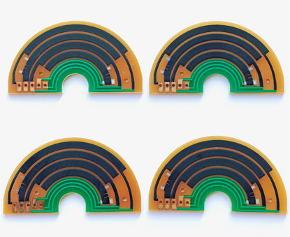
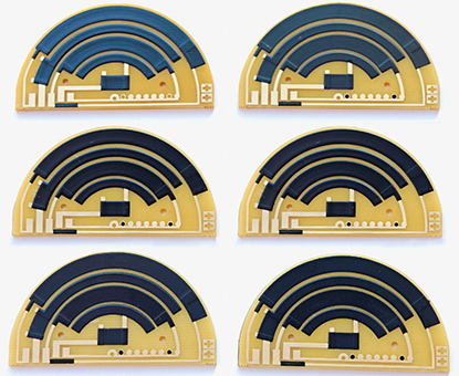
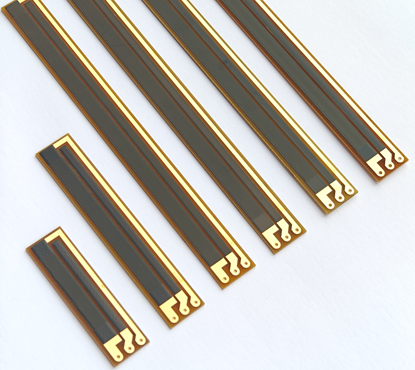
1, Flexible Thick Film PCB : |
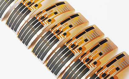 |
Flexible Thick Film PCBs, also known as Flex Thick Film PCBs, are specialized hybrid circuits that use flexible polyimide (PI) and polyester (PET) as substrates, with the thick film screen-printing process applied to print conductive, resistive, and insulating pastes onto these substrates, resulting in flexible thick film PCBs with integrated resistors, capacitors, or sensors. Flexible Thick Film PCBs offer single and double-sided flexible thick film circuits for low current applications. By using the screen-printing process to print various types of pastes, hybrid circuits can be created cost-effectively. The configurations of thick film flexible PCBs are also available in different processes, such as etching copper images on one side and printing paste patterns on the other side, double-sided etching copper patterns, or double-sided conductive silver paste printing. |
Flexible Thick Film PCBs are utilized across multiple industries, including automotive, aerospace, medical devices, and consumer electronics. It is used in various applications such as flexible displays, membrane switches, sensors, wearable devices, and more. At Panda-PCB's Thick Film Solution, We offer three types of Thick Film Flexible PCB tailored to different applications, include Flexible Linear Potentiometers, Flexible Sensors (Flexible Electronics), Printed Flexible Electronic and Flexible Heaters (PI and PET). |
|
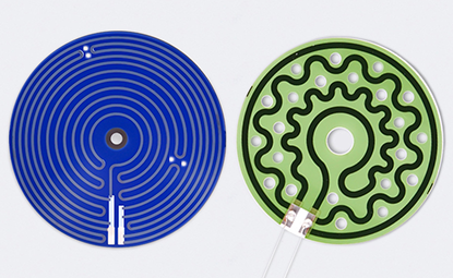
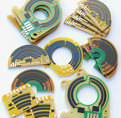
2, Thick Film Potentiometer PCB : |
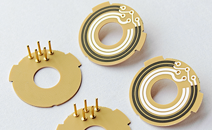 |
Thick Film Potentiometer PCBs are specialized electronic components that combine variable resistors with printed circuit boards. It uses thick film technology, where different types of pastes, such as conductive, resistive, and insulating materials, are sequentially applied onto PI, FR4, or ceramic PCBs, then subjected to high-temperature sintering and laser trimming, resulting in precise, reliable potentiometers that provide efficient and customizable solutions for various electronic systems. Thick Film Potentiometer PCBs can achieve all the functions of linear potentiometer, rotary potentiometer and logarithmic taper potentiometer, which is equivalent to transplanting or integrating the potentiometer module directly onto the PCB surface. It can not only effectively save the assembly space of the products, but also provide a variety of options for product developers. |
● Linear Potentiometer PCB : A resistive carbon layer is printed on the surface of the PCB as the resistor element, consisting of a linear slider that controls the position of the wiper, which slides along the thick film resistor printed on the PCB in a linear manner. ● Rotary Potentiometer PCB : Printing a resistive carbon layer on the surface of a PCB as the resistor element, the most common type of potentiometer, They use a rotary knob to move the wiper around the thick film resistor printed on the PCB. |
|
3, Thick Film Heaters / Thick Film Heating Elements : |
 |
Thick Film Heaters are advanced and efficient heating elements that employ advanced thick film technology to precisely print dielectric, resistive, conductive, and insulating materials onto flexible PI, ceramic, or stainless steel substrates, with a process involving precise material mixing, layer-by-layer printing, high-temperature sintering, and laser trimming to optimize structure and performance, ensuring excellent high-temperature, wear, and corrosion resistance for stable long-term operation in harsh environments. Thick Film Heating Elements are highly versatile and widely used in industries such as automotive, aerospace, electronics, medical devices, and renewable energy. Their precise heat distribution and compact design make them ideal for applications like temperature sensors, thermal management and solar thermal systems. With excellent durability, energy efficiency, and uniform temperature control. |
At Panda-PCB's Thick Film Heating Solution, We provides three types of thick film heaters based on different substrates, Like flexible polyimide, metal core and ceramic substrate; So we called them as Flexible Heaters, Stainless Steel-Thick Film Heaters, and Ceramic-Thick Film Heaters. |
|
4, Thick Film Ceramic Resistors / Thick Film Ceramic PCBs : |
 |
Thick Film Ceramic Resistors are precision electronic components designed to control the flow of current in a circuit, serving functions such as circuit regulation, power distribution, and protection, and are manufactured using thick film technology where resistive and conductive materials are printed onto a ceramic substrate, followed by high-temperature sintering and laser trimming to form a stable, durable, reliable, and customizable resistor element on the surface of the ceramic substrate. Thick Film Ceramic PCBs are built with ceramic substrates like alumina or aluminum nitride, which offer superior thermal conductivity, mechanical strength, and chemical resistance compared to the traditional FR4 substrate found in standard PCBs. These ceramic materials make the PCBs highly suitable for applications in environments that demand high thermal management and resistance to harsh chemicals, etc. |
Thick Film Ceramic Resistors are used in various electronic devices, including power supplies, amplifiers, and control circuits. Their durability makes them ideal for automotive and industrial equipment, as well as consumer electronics like televisions, computers, and communication devices. Their ability to handle different power ratings and tolerance levels makes them versatile across multiple sectors, contributing to the longevity and reliability of many products. |
|
5, Thick Film Circuits / Thick Film Hybrid Circuits : |
 |
Thick Film Circuits are customizable and highly reliable electronic circuits that use thick film technology to print conductive, resistive, and insulating materials onto ceramic substrates, followed by high-temperature sintering and laser trimming to directly form durable and precise electrical components on the substrate, making them known for their high integration, excellent environmental durability, and cost-effectiveness, thus an ideal choice for demanding applications. Thick Film Hybrid Circuits enables the creation of resistors, capacitors, conductive traces, and other passive components directly on the ceramic substrate, eliminating the need for separate discrete components. These conductive elements need be fired in tightly monitored temperature controlled, multi-zoned furnaces, binding the conductive paste to the base material and becoming an integral part of the thick film hybrid circuits. |
Thick Film Circuits are used across industries requiring performance, durability, and compactness, such as automotive electronics, medical devices, telecommunications, and industrial control systems. In automotive applications, they are found in engine control units and sensor systems. In medical devices, they provide precision and resistance to external factors. They are also essential in telecommunications for signal processing and in industrial control systems for automation and machinery reliability. |
|
6, Hybrid Microcircuits / Hybrid Integrated Circuits : |
 |
Hybrid Microcircuits are a type of microcircuit that use a combination of screen printing and firing techniques to print conductive, resistive, and dielectric materials on a ceramic substrate. The process involves printing successive layers of thick film pastes onto the substrate to form individual components such as resistors, capacitors, and conductive traces. These layers are then fired in a high-temperature furnace to create a solid, permanent structure. Hybrid Integrated Circuits are also a type of electronic circuit that combines multiple components on one substrate, typically ceramic or quartz. It consists of a combination of miniature passive and active electronic components like resistors, capacitors, transistors, diodes, and inductors that are mounted onto a single package by using small metallic wires or conductive pathways to connect them together. |
Hybrid Microcircuits serve as components on PCBs in the same way as integrated circuits (ICs) do. The difference between the two types of devices is in how they are constructed and manufactured. These small custom packages result in higher performance modules than may be available through the application of typical commercially available components. In military, automotive, and space applications, numerous integrated circuits, transistors, and diodes, in their die form, would be placed on either a hybrid microcircuit. |
|
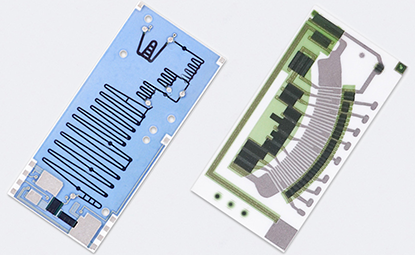
7, Thick Film Sensors : |
 |
Thick Film Sensors are sensor elements manufactured using thick film technology, widely used for detecting and measuring a range of physical parameters such as position, angle, temperature, pressure, humidity, and gas concentration; these sensors utilize a cost-effective manufacturing process where thick film materials are applied to the surface of a circuit board, forming functional sensing elements, ensuring stability and durability. Thick Film Sensors are characterized by high reliability, low manufacturing costs, and customizable functionality. Thanks to the nature of thick film technology, the sensor elements can achieve large sizes and high resistance to interference without compromising accuracy. Additionally, thick film sensors can be tailored to meet different application needs, detecting various physical or chemical stimuli, such as changes in temperature, pressure, humidity, or the presence of specific chemicals. |
Thick Film Sensors operate based on the principle of resistance change. The thick film material applied to the sensor's surface undergoes physical property changes in response to environmental factors such as temperature, pressure, or humidity, resulting in variations in resistance. For example, when external pressure changes, the thick film material inside the sensor may deform or compress, leading to a corresponding change in resistance. The sensor's circuit system continuously monitors these changes and outputs signals that reflect the changes in environmental parameters. |
|
Typical Applications of Thick Film Resistor PCB : |
1. Power Electronics: In power electronics, Thick Film Resistor PCBs are used in power supplies, inverters, converters, and energy storage systems. They help in current sensing, voltage dividing, and power management functions. 2. Aerospace and Defense: Thick Film Resistor PCBs are employed in aerospace and defense applications, such as avionics systems, radar systems, communication equipment, navigation systems, and military-grade electronics. They offer stability, accuracy, and resistance to harsh environmental conditions. |
|
 |
3. Automotive Electronics: Thick Film Resistor PCBs play a vital role in automotive electronics, where they are used in Power Modules, Throttle Valve Sensor, Ignition Module, Voltage Regulator, Fuel Level Sensor, and Control Modules. They provide accurate resistance values and stability in harsh conditions, ensuring reliable performance. 4. Telecommunications: Thick Film Resistor PCBs are essential in telecommunications equipment such as routers, switches, base stations, and network infrastructure devices. They help in signal conditioning, impedance matching, and voltage regulation. 5. Renewable Energy Systems: Thick Film Resistor PCBs play a role in renewable energy systems, including solar power inverters, wind turbine control systems, and battery systems. They contribute to efficient power conversion and energy management. 6. Consumer Electronics: Thick Film Resistor PCBs are commonly used in consumer electronics such as smartphones, tablets, laptops, televisions, audio control potentiometer, and gaming consoles. They help regulate current flow and voltage levels, ensuring proper functioning of the devices. |
7. Medical Devices: Medical devices require high precision and reliability, making Thick Film Resistor PCBs an ideal choice. They are used in various medical equipment, including patient monitoring systems, diagnostic devices, imaging equipment, and surgical instruments. 8. Industrial Control Systems: Thick Film Resistor PCBs are utilized in industrial control systems for measurement, monitoring, and control purposes. They can be found in programmable logic controllers (PLCs), motor control units, robotics, power supplies, and industrial automation equipment. |
|
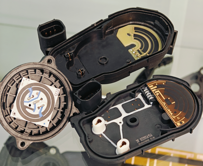
Application of Thick Film Resistor PCB in Automotive Electronics : |
Thick Film Resistor PCBs find diverse applications in automotive electronics due to their reliability, precision, and ability to withstand harsh operating conditions. Let's elaborate on the specific applications: 1, Throttle Position Sensor: Thick film resistor PCBs are utilized in throttle valve sensors to provide accurate and reliable feedback on the position of the throttle valve, enabling the engine control unit to adjust fuel injection and optimize engine performance. 2, Fuel Level Sensor: Thick film resistor PCBs are integrated into fuel level sensors to accurately measure the fuel level in the tank. The resistive elements provide the basis for precise fuel level indication on the vehicle's dashboard. |
|
 |
3, Power Modules: Thick film resistor PCBs are used in power modules for controlling and managing power distribution within the vehicle. They are employed in systems such as motor control units, battery management systems, and power converters, where precise and reliable resistive elements are required for power handling. 4, Ignition Module: In ignition modules, thick film resistor PCBs are employed for voltage dividers, pull-up or pull-down resistors, and other circuit functions essential for ignition system operation. 5, Voltage Regulator: Thick film resistor PCBs play a crucial role in voltage regulation by providing precision resistive elements for voltage divider circuits and feedback networks in automotive voltage regulator modules. 6, Displays and Instrumentation: In automotive displays and instrumentation panels, thick film resistor PCBs are employed for voltage dividers, pull-up or pull-down resistors, and other circuitry essential for controlling and interfacing with various display and control elements. |
7, Heating Elements: Thick film resistor PCBs are used as heating elements in applications such as seat heaters, window defrosters, and other heating systems within the vehicle cabin, providing efficient and controlled heating functionality. 8, EV and HEV (Electric Vehicle and Hybrid Electric Vehicle): Thick film resistor PCBs are integral to the electrical systems of electric and hybrid vehicles, where they are used in power control units, battery management systems, regenerative braking systems, and other critical electronic components. The application of thick film resistor PCBs in automotive electronics spans a wide range of functions critical to vehicle operation, including power management, sensor interfaces, heating systems, and control circuitry for electric and hybrid vehicles. Their reliability and precision make them well-suited for the demanding requirements of automotive applications. |
|
Advantages of Thick Film Resistor PCB : |
1, Higher Reliability: 2, Wider Temperature Range and Excellent Thermal Dissipation: |
|
 |
3, Higher Precision on Resistors: 4, Low Coefficient of Thermal Expansion (Low-CTE): 5, More Compact, Efficient Package, Economical: 6, Low Failure Rate: |
7, High Frequency: 8, Excellent Flexibility: |
|
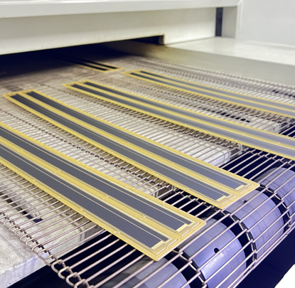
Key Manufacturing Processes of Thick Film Resistor PCB : |
1, Thick Film Substrate Preparation: 2, Preparation of Thick Film Pastes: |
|
 |
3, Screen Printing Process: 4, Drying: 5, Firing/Sintering: |
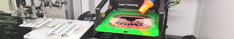
6, Multilayer-Thick Film Substrates with Crossover Conductors: 7, Laser Trimming for Precision: |
|
 |
8, Protective Coatings: 9, Surface Preparation: 10, Inspection and Quality Control: |
11,Assembly and Integration: 12, Testing and Final Inspection: 13, Packaging and Labeling: |
|
Linearity Definition of Thick Film Resistor PCB : |
The linearity of a Thick Film Resistor PCB refers to how closely the resistance changes in relation to the movement of the wiper or slider along the resistor's surface. In other words, it measures the degree to which the resistance follows a linear relationship with the position of the wiper. A resistor with high linearity will exhibit a consistent and predictable change in resistance as the wiper moves, adhering closely to a linear relationship. Conversely, a resistor with poor linearity may deviate from this linear relationship, resulting in non-linear changes in resistance across its range. Linearity is crucial in applications such as potentiometers or position sensors, where precise and stable voltage outputs are required. 1, Linearity is an important characteristic for applications where precise and accurate position sensing is required. It ensures that the potentiometer provides a consistent and predictable response to changes in position, making it suitable for applications such as volume control, position control, and user interface input devices. |
|
 |
2, Linearity refers to the extent to which the output characteristic curve of a sensor deviates from an ideal straight line. It is typically measured by the maximum deviation from this ideal line in relation to the applied voltage, and expressed as a percentage. There are three common types of nonlinearities specified for potentiometer sensors: ● Independent Linearity: This type of linearity considers the deviation of the output characteristic curve independently, without reference to any other variables or conditions. ● Absolute Linearity: Absolute linearity takes into account the overall deviation of the output characteristic curve, considering all possible factors and conditions. ● Terminal Linearity: Terminal linearity focuses on the deviation of the output characteristic curve at the ends or terminals of the sensor's measurement range. |
3, When specifying the required type of linearity and linearity deviation for a potentiometer sensor, it is important to customize them for each specific application. If a percentage of linearity is provided without additional information, it is typically understood to refer to independent linearity. 4, The typically specify the linearity of a potentiometer as a percentage of the maximum deviation from a perfectly linear response. For example, a potentiometer with a linearity specification of ±1% means that the actual output may deviate from a perfect linear relationship by up to 1% of the full-scale range. If you need more tighter linearity, we can control it to be 0.25% or 0.5% by laser trimming process, but it costs higher as well. |
|
Factors Ensuring Voltage Stability in Thick Film Resistor PCB: |
Thick Film Resistor PCBs are influenced by several key factors that determine the stability of voltage output. Understanding these factors is essential for designing circuits that demand precise control over their electrical characteristics. Here are the primary factors to consider: 1, Linearity: Linearity refers to the ability of a resistor to maintain a constant resistance value across its operating range. In an ideal scenario, the resistance should not change with varying voltage levels, ensuring that the output remains stable and predictable. Non-linear behavior can introduce distortions or variations in the voltage output, affecting the performance of the electronic device. |
|
 |
2, Temperature Coefficient of Resistance (TCR): TCR is a measure of how much a resistor's value changes with temperature. It is expressed in parts per million per degree Celsius (ppm/°C). A low TCR means that the resistor's value remains relatively stable across a wide range of temperatures, contributing to the overall stability of the voltage output. High TCR values indicate that the resistor's resistance might vary significantly with temperature changes, potentially leading to unstable voltage outputs under different operating conditions. 3, Long-term Stability: This refers to the ability of a resistor to maintain its resistance value over time. Factors affecting long-term stability include aging, exposure to environmental conditions (such as humidity and temperature extremes), and mechanical stress. High-quality thick film resistors are designed to minimize these effects, ensuring that their resistance values change very little over their intended lifespan, thereby maintaining stable voltage outputs. |
4, Load Life Stability: This factor considers how the resistor's performance changes with prolonged use under load. Continuous electrical loading can lead to changes in the resistor's structure, affecting its resistance. A resistor with good load life stability will exhibit minimal changes in resistance value when subjected to its rated power over time. 5, Noise: Electrical noise in resistors can also affect the stability of voltage output. Noise refers to small, random fluctuations in the voltage or current. In precision applications, even a small amount of noise can be problematic. Thick Film Resistor PCBs can generate noise due to various mechanisms, including the grain structure of the conductive material and the interface between the conductive material and the substrate. Choosing resistors with low noise characteristics is essential for applications requiring stable voltage outputs. 6, Environmental Factors: Exposure to harsh environmental conditions such as high humidity, corrosive atmospheres, or extreme temperatures can degrade the performance of resistors over time. High-quality Thick Film Resistor PCBs are designed and tested to withstand these conditions without significant changes in their resistance values, ensuring stable voltage outputs in a wide range of environments. |
|
What's Important Role of Linearity in Thick Film Resistor PCB ? |
● Linearity of linear and rotary potentiometers or position sensors pertains to how closely the resistance changes relative to the movement of the wiper or slider along the resistor's surface. It quantifies the extent to which the resistance maintains a linear correlation with the position of the wiper. A resistor with high linearity will exhibit a consistent and predictable change in resistance as the wiper moves, adhering closely to a linear relationship. Conversely, a resistor with poor linearity may deviate from this linear relationship, resulting in non-linear changes in resistance across its range. ● A smaller linearity value indicates that the change in resistance across the potentiometer's entire range is more consistent, adhering closely to a linear relationship. This consistency results in a more precise and stable voltage (or signal) output. In simpler terms, a lower linearity value means that minor positional adjustments of the wiper lead to proportional and predictable changes in output voltage. |
|
 |
● Conversely, a larger linearity value suggests potential deviations from a linear resistance change as the wiper moves, introducing non-linearities and inconsistencies in the voltage output, which diminish precision and stability. ● Therefore, achieving a lower linearity value in a linear potentiometers or rotary potentiometer is crucial for ensuring accurate and stable voltage outputs, thus guaranteeing reliable performance across various applications. ● During our production of potentiometer PCB or position sensor PCB, a one-time carbon printing process can achieve a standard resistance tolerance of ±10% with a linearity of ±1.0% without laser trimming. If customers require linearity of less than 1.0% (e.g., 0.5% or 0.25%), then laser trimming becomes necessary for adjusting linearity. For example, under our normal processes, a one-time carbon printing process can achieve a standard resistance tolerance of : |
If the customer requires a linearity of <1.0%, then the resistance tolerance must be adjusted to ±15% or +/-20%, Then it should be : ● When using laser trimming to achieve lower linearity, the resistance value continuously fluctuate along with the entire process of laser trimming (the resistance increases over time). Therefore, in such conditions, it becomes unreasonable to demand a high precision (tolerance) controlling of the resistance value , as it hinders the attainment of better linearity. On the contrary, as the consistency of linearity improves, it is generally preferred to relax the resistance tolerance range and ensuring the manufacturability of laser trimming. In summary, ensuring good linearity takes precedence over precise control of the resistance value in the production of potentiometers. ● It's important to note that while resistance tolerance is a factor in determining a resistor's overall precision, But it is not the primary determinant of voltage output stability. In essence, if the resistor design incorporates linear functionality, controlling a lower linearity tolerance becomes more critical than managing resistance tolerance. |
|
How to Calculate the Linearity of Thick Film Resistor PCB : |
1, Determine the Resistance Value: Measure the resistance value of the Thick Film Resistor PCBs under test conditions. This can be done using a multimeter or other suitable measuring equipment. 2, Apply Different Voltages: Apply a range of different voltages across the resistor and measure the resulting currents. Ensure that the applied voltages are within the specified operating range of the resistor to avoid damaging it. |
|
 |
3, Plot Voltage vs. Current Graph: Plot a graph with voltage on the x-axis and current on the y-axis using the measured values. This graph represents the current-voltage (I-V) characteristic of the resistor. 4, Calculate Linearity: The linearity of the Thick Film Resistor PCB can be assessed by analyzing the I-V curve. A perfectly linear resistor would exhibit a straight line on the graph, indicating a constant resistance value across different voltage levels. However, in practical scenarios, resistors may deviate from perfect linearity. Calculate the deviation of the plotted curve from a straight line to quantify the linearity. 5, Use Regression Analysis: Perform regression analysis on the plotted data to determine the best-fit line and evaluate how closely the measured data points align with this line. Statistical methods such as coefficient of determination (R-squared) can be used to quantify the linearity. |
6, Assess Nonlinear Effects: It's also important to inspect any nonlinear effects, such as temperature-dependent resistance variations, that may influence the overall linearity of the Thick Film Resistor PCBs. By following these steps and analyzing the I-V characteristics, you can calculate and evaluate the linearity of a Thick Film Resistor PCB, providing insights into its performance under varying voltage conditions. |
|
Multi-Wire Wipers Used For Thick Film Resistor PCB : |
 |
Multi-Wire Wipers are crucial components designed to transmit voltage and signals. They perform linear or rotational sliding over the surfaces of resistive materials (thick film resistors) to adjust resistance values and act as contact elements in voltage dividers. Wiper design is extremely critical for the efficiency and life of the sensor assembly, When designing the wiper, it is very important to consider contact resistance, working-hight (load), repeatability, hysteresis, the resistive material used, and in particular, the wiper material itself, its shape and the wiper pressure. We also provided custom Multi-Wire Wipers (Contact) for customer if needs, we can manufacture the wipers according to customer's design requirements or specification, For more information about wipers, Please refer to Multi-Contact Wipers. |
Why Choose PANDA PCB For Thick Film Resistor PCB ? |
At PANDA PCB Group - Thick Film Technology, we offer accurate, reliable, and cost-effective solutions for custom thick film circuit board manufacturing. Our state-of-the-art technology allows us to precisely screen print conductive, resistive, and insulating pastes which are then fused at high temperatures onto FR4, flexible material, ceramic, and metal core substrates. By using different pastes, we can produce both conductive tracks and resistors that can be customized and laser-trimmed to a high level of accuracy, ensuring an exact choice of value without any compromise in design. Our process results in a reliable, cost-effective thick film resistor PCB that meets your specific requirements and specifications. |
|
 |
● Panda PCB has over 20 years of experience in the field of thick film resistor PCB. Our team of engineers possesses extensive knowledge and expertise in designing and manufacturing these circuits, ensuring that our products are of the highest quality. ● Panda PCB is committed to providing high-quality products to their customers. We use only the best materials and follow strict quality control processes to ensure that each thick film hybrid circuit meets or exceeds industry standards. This dedication to quality translates into durable and reliable products that are built to last. ● We offers customization options to meet the specific needs of their clients. We understand that each application may have unique requirements, and we are willing to work with our customers to develop a custom thick film solution that fits their needs. ● Panda PCB is a reputable and reliable provider of thick film resistor PCB. Our expertise, focus on quality, customization options, advanced manufacturing facilities, and commitment to customer satisfaction make them an excellent choice for anyone in need of thick film circuits, thick film resistors and thick film heaters. |
Design Guidelines of Thick Film Resistor PCB : |
We compiled a Thick Film Resistor PCB-Design Guidelines as attached for you to download, It is to better support our customers' needs in designing and applying Thick Film Resistor PCBs, This guide covers detailed information on product solutions, engineering design specifications, material properties, available manufacturing processes, and more. We hope that this guide will assist customers in standardizing their design process while ensuring the manufacturability of the design data, ultimately improving product reliability and production efficiency. Customers are encouraged to refer to the guide when designing Thick Film Resistor PCBs to ensure adherence to best practices. |
Capabilities of Thick Film Resistor PCB are As Follows : |
1, Engineering Specification of Thick Film Resistor PCB :
Items : |
Typical Values |
Advanced Capabilities |
1, Substrates : |
FR4, Ceramic ( AI203, ALN, BeO, ZrO2), Polyimide (Flexible PI), Stainless Steel (SUS304), Mica |
FR4, Ceramic ( AI203, ALN, BeO, ZrO2), Polyimide (Flexible PI), Stainless Steel (SUS304), Mica |
2, Conductor (Paste) Materials : |
Copper, Silver , Gold , Silver-Palladium, Palladium-Gold, Platinum-Silver, Platinum-Gold |
Copper, Silver , Gold , Silver-Palladium, Palladium-Gold, Platinum-Silver, Platinum-Gold |
3, Thick Film Carbon Thickness (Height) : |
15um +/-5 um |
30um +/-5 um |
4, Conductor Thickness (Height) : |
12um+/-5um |
20um+/-5um |
5, Min Width of Thick Film Line : |
0.30 mm +/-0.05 mm |
0.20 mm +/-0.05 mm |
6, Min Space of Thick Film Line : |
0.30 mm +/-0.05 mm |
0.20 mm +/-0.05 mm |
7, Min Overlap (Carbon to Conductor) : |
No less than 0.25mm |
0.20mm (Minimum) |
8, Sheet Resistivity (ohms/square): |
Printed resistors in milli ohm to mega ohm range (Customizable) with tolerances of 1-10% are fabricated and protected with overglaze materials. |
Printed resistors in milli ohm to mega ohm range (Customizable) with tolerances of 0.5-10% are fabricated and protected with overglaze materials. |
9, Resistor Value Tolerance (ohms) : |
+/-10.0% (Standard) (Customizable) |
+/-0.5% (Laser trimming) |
10, Linearity : |
+/-1.0% (Standard) (Customizable) |
+/-0.2 ~ +/-0.5% (Laser trimming) |
11, Synchronism of Double Channels : |
+/-2.0% (Standard) (Customizable) (Potentiometers) |
+/-1.0% (Laser trimming) (Potentiometers) |
12, Durability of Carbon Ink (Life time) : |
0.5 Million (Min), 2.0 Million (Standard) |
5.0-10.0 Million (Max) with Surface Polishing |
13, Working Temperature : |
- 40ºC /+150ºC |
- 40ºC /+180ºC |
2, Optional Processes of Thick Film Resistor PCB (Ceramic Substrates) :
Metalization Types : |
Thick Film Substrates (Screen-Printed) |
Thin Film Substrates (Photo-Imaged) |
|||
Process Types : |
TFM Capabilities |
HTCC / LTCC Capabilities |
DBC Capabilities |
DPC Capabilities |
AMB Capabilities |
Layer Counts : |
1, 2, 3, 4, 5, 6 Layers |
1, 2, 4, 6, 8, 10, 12 Layers |
1, 2 Layers |
1, 2 Layers |
1, 2 Layers |
Max Board Dimension : |
200*230mm |
200*200mm |
138*178mm |
138*190mm |
114*114mm |
Min Board Thickness : |
0.25mm |
0.25mm |
0.30mm~0.40mm |
0.25mm |
0.25mm |
Max Board Thickness : |
2.2mm |
2.0mm |
1L: 1.6mm; 2L 2.0mm |
2.0mm |
1.8mm |
Conductor Thickness : |
10um - 20um |
5um - 1500um |
1oz - 9oz |
1um - 1000um |
1oz- 22oz |
Min Line Width/Space : |
8/8mil (0.20/0.20mm) |
6/6mil (0.15/0.15mm) |
10/10mil (0.25/0.25mm) |
6/6mil (0.15/0.15mm) |
12/12mil (0.30/0.30mm) |
Substrates Types : |
AI203, ALN, BeO, ZrO2 |
AI203, ALN, BeO, ZrO2 |
Al2O3, AlN, ZrO2, PbO, SiO2, ZTA, Si3N4, SiC, Sapphire, Polycrystalline Silicon, Piezoelectric Ceramics |
Al2O3, AlN, ZrO2, PbO, SiO2, ZTA, Si3N4, SiC, Sapphire, Polycrystalline Silicon, Piezoelectric Ceramics |
AI203, ALN, BeO, ZrO2, Si3N4 |
Min Hole Diameter : |
4mil (0.15mm) |
4mil (0.15mm) |
4mil (0.1mm) |
4mil (0.1mm) |
4mil (0.1mm) |
Outline Tolerance : |
Laser: +/-0.05mm; Die Punch: +/-0.10mm |
Laser: +/-0.05mm; Die Punch: +/-0.10mm |
Laser: +/-0.05mm; Die Punch: +/-0.10mm |
Laser: +/-0.05mm; Die Punch: +/-0.10mm |
Laser: +/-0.05mm; Die Punch: +/-0.10mm |
Substrate Thickness : |
0.25, 0.38, 0.50, 0.635, 0.80,1.0, 1.25, 1.5, 2.0mm, Customizable |
0.25, 0.38, 0.50, 0.635, 0.80,1.0, 1.25, 1.5, 2.0mm, Customizable |
0.25, 0.38, 0.50, 0.635, 0.80,1.0, 1.25, 1.5, 2.0mm, Customizable |
0.25, 0.38, 0.50, 0.635, 0.80,1.0, 1.25, 1.5, 2.0mm, Customizable |
0.25, 0.38, 0.50, 0.635, 0.80,1.0, 1.25, 1.5, 2.0mm, Customizable |
Thickness Tolerance : |
0.25-0.38: +/-0.03mm; 0.50-2.00: +/-0.05mm |
0.25-0.38: +/-0.03mm; 0.50-2.00: +/-0.05mm |
0.25-0.38: +/-0.03mm; 0.50-2.00: +/-0.05mm |
0.25-0.38: +/-0.03mm; 0.50-2.00: +/-0.05mm |
0.25-0.38: +/-0.03mm; 0.50-2.00: +/-0.05mm |
Surface Treatment : |
Ag, Au, AgPd, AuPd |
Ag, Au, AgPd, AuPd, Mn/Ni |
OSP/Ni Plating, ENIG |
OSP/ENIG/ENEPIG |
OSP/ENIG/ENEPIG |
Min Solder PAD Dia : |
10mil (0.25mm) |
10mil (0.25mm) |
8mil (0.20mm) |
6mil (0.15mm) |
8mil (0.20mm) |
3, Ceramic Substrates of Thick Film Resistor PCB :
Substrates : |
Alumina (Al2O3) |
Aluminum Nitride (AlN) |
Beryllium Oxide (BeO) |
Zirconium Dioxide (ZrO2) |
Max Application Temperature : |
662 - 1832 |
1832 |
2300 |
2432 |
Max Power Density (W/in²): |
75 |
1010 |
250 |
300 |
Max Ramp Up Speed (°F/sec): |
122 |
572 |
400 |
350 |
Thermal Conductivity (W/mK): |
20-35 |
180-220 |
200-300 |
2.0-5.0 |
Density (g/cm³): |
3.75 |
3.26 |
2.8 |
5.9 |
Dielectric Loss: |
0.0001 - 0.001 |
0.0001 - 0.0005 |
0.0001 - 0.0002 |
0.0005 - 0.001 |
Dielectric Constant: |
9.4 - 10.2 |
8.5 - 9.0 |
6.0 - 7.0 |
25 - 30 |
CTE, ppm/ºC: |
6.0 - 8.0 |
4.0 - 5.0 |
7.0 - 9.0 |
10.0 - 11.0 |
Substrate Thickness (mm): |
0.25 - 2.0 |
0.25 - 2.0 |
0.25 - 2.0 |
0.25 - 2.0 |
Typical Max. Dimension (inch): |
6 x 12 |
5 x 11 |
6 x 6 |
4 x 4 |
Theoretical Total Wattage (W): |
5400 |
55000 |
15000 |
20000 |
4, Conductive Paste of Thick Film Resistor PCB :
Paste ( Materials) : |
Conductor Width/Space |
Soldering / Bonding |
Gold : |
8/8mil (0.20/0.20mm) |
Gold is a good conductor material and allows thermo-compression gold wire bonding and eutectic die attachment. It is, of course, costly and has poor solderability. |
Silver : |
8/8mil (0.20/0.20mm) |
Soldering & Silver is lower in cost, and solderable, but is not leach-resistant with tin/lead solders.More seriously, silver atoms migrate under the influence of DC electric fields, both causing short-circuits and reacting with many of the resistor paste formulations. |
Platinum-Silver : |
6/6mil (0.15/0.15mm) |
Soldering & Surface Mount, Palladium and platinum alloyed to the gold and silver produce good conductor pastes,with good adhesion to the substrate, good solderability, and moderately good wire bonding characteristics. Copper and nickel are examples of materials that have been proposed for paste systems as substitutes for noble metals. |
Palladium-Silver : |
8/8mil (0.20/0.20mm) |
Soldering & Surface Mount ,Solderable, Wire bondable, (good aged adhesion general purpose), Silver-palladium conductor inks are the most commonly used materials, with both price and performance (primarily resistance to solder) increasing with palladium content. |
Platinum-Gold : |
6/6mil (0.15/0.15mm) |
Soldering & Au or Al Wire Bonding, Solderable (excellent aged adhesion with no migration). |
Palladium-Gold : |
8/8mil (0.20/0.20mm) |
Soldering & Au or Al Wire Bonding, Wire bondable. |
5, Resistive Paste of Thick Film Resistor PCB :
Performances : |
Common Values/Range |
Description |
Resistance Value : |
1Ω to several MΩ |
The resistance value depends on the type and ratio of carbon black, typically ranging from 1Ω to Mega ohm. |
Resistance Tolerance : |
±1% to ±10% |
High-precision resistors can achieve ±0.1% tolerance used laser trimming process. |
Temperature Coefficient (TCR) : |
±50ppm/°C to ±200ppm/°C |
High-quality resistive paste should have a low TCR, preferably below ±100ppm/°C. |
Stability : |
≤1% |
Resistors must undergo high-temperature aging and humidity tests to ensure stability. |
Sintering Temperature : |
850°C to 950°C |
The sintering temperature for carbon paste depends on material properties, typically in this range. |
Conductivity : |
10⁶ S/m to 10⁸ S/m |
Conductivity depends on the type and ratio of carbon black, affecting resistance precision and stability. |
Surface Smoothness : |
Ra≤ 1 μm |
The surface must be free of cracks, bubbles, and non-uniform layers to ensure good mechanical and electrical properties. |
Insulation Resistance : |
≥10⁹ Ω |
Carbon paste should have good insulation properties to avoid leakage or short circuits. |
Mechanical Strength : |
≥100 MPa |
The resistive layer must have good compressive and bending strength to ensure the reliability of the resistor. |
Volatility : |
Solvent residue ≤ 1% |
High volatility solvents help with even coating and drying, but excessive volatility may affect electrical performance. |
Oxidation Resistance : |
>1000 hours |
High-quality carbon paste should have strong oxidation resistance to extend the service life. |
Humidity Resistance : |
≥1000 hours |
Resistors should be able to withstand high-humidity conditions to ensure long-term stable performance, no significant changes. |
6, Dielectric Paste of Thick Film Resistor PCB :
1, High Dielectric Strength: The dielectric paste should have a high dielectric strength to withstand high electric fields and prevent electrical breakdown. Typical values range from several hundred to several thousand volts per mil (V/mil). 2, Low Temperature Coefficient of Resistance (TCR): The TCR indicates the change in resistance with temperature. For stable resistor performance, a low TCR is desirable. Values of around ±100 ppm/°C are common for thick film resistor pastes. 3, Good Insulation Resistance: The paste should exhibit high insulation resistance to prevent current leakage and maintain electrical isolation between the resistive layer and other components on the PCB. Typical insulation resistance values are in the range of several megaohms to gigaohms. 4, Low Moisture Absorption: Low moisture absorption is crucial to maintain the stability of the resistive layer and prevent changes in resistance due to moisture ingress. A moisture absorption rate of less than 0.5% is desirable. 5, High Adhesion Strength: The paste should have good adhesion properties to ensure it adheres well to the substrate and does not delaminate or detach during operation or manufacturing processes. Adhesion strength is typically measured in pounds per square inch (psi) or Newtons per square millimeter (N/mm²). |
7, Insulating Paste of Thick Film Resistor PCB :
The insulating paste, also known as the passivation layer, is an essential component of thick film resistor PCBs. It serves to protect the resistive layer and other elements of the PCB from environmental factors and ensure long-term performance. Here are some key points about the protective paste: 1, Purpose: The insulating paste is applied over the resistive layer of the thick film resistor PCB to provide protection against moisture, contaminants, and physical damage. It acts as a barrier, preventing external factors from degrading the resistive properties of the PCB. 2, Material Composition: The insulating paste is typically made of a glass or ceramic material that offers excellent insulation and resistance to corrosion, oxidation, and chemical attack. It may contain additives to enhance its mechanical strength and thermal stability. Normally, a Resin Paste (Solder Mask) is screen-printed onto an FR4 PCB as a protective layer. For custom thick film heating elements, non-metallic materials called Overglazes (Glass Glaze) are printed as a protective layer. 3, Application: The insulating paste is printed onto the PCB using screen printing techniques. It is applied in a uniform layer over the resistive layer, covering the entire surface to ensure comprehensive protection. 4, Insulation: The insulating paste provides electrical insulation, preventing unintended electrical connections between the resistive layer and other conductive elements on the PCB. This insulation is crucial for maintaining the accuracy and reliability of the resistor's resistance value. 5, Environmental Protection: The insulating paste shields the resistive layer from moisture, humidity, dust, and other contaminants that could compromise its performance. It helps to maintain the stability and longevity of the thick film resistor under various operating conditions. |