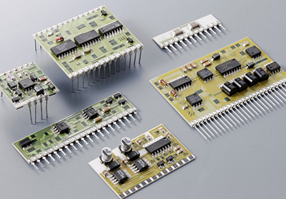
Thick Film Hybrid Circuits
Thick Film Hybrid Circuits are highly reliable electronic circuits made by combining thick-film technology with ceramic substrates, involving the printing of conductive, resistive, precious metal, or insulating pastes onto alumina or aluminum nitride substrates, followed by processes like high-temperature sintering, laser trimming, photolithography, and bonding encapsulation, which integrate specific components such as resistors, capacitors, sensors, or heaters, widely applied in automotive, aerospace, medical, and telecommunications industries, offering advantages in customizability, and high power handling. Thick Film Hybrid Circuits enables the creation of resistors, capacitors, conductive traces, and other passive components directly on the ceramic substrate, eliminating the need for separate discrete components. These conductive elements need be fired in tightly monitored temperature controlled, multi-zoned furnaces, binding the conductive paste to the base material and becoming an integral part of the thick film hybrid circuits. Thick Film Hybrid Circuits are known for their stability and durability, making them suitable for various operating conditions and environments. The thick film material provides good adhesion to the substrate and exhibits excellent resistance to temperature variations, humidity, and mechanical stress. Hybrid Circuits offers several advantages, including cost-effectiveness, compactness, and good electrical performance. Main Features of Thick Film Hybrid Circuits : |
 |
|
 |
1, Versatile Applications: Thick Film Hybrid Circuits find applications in various industries, including commercial, industrial, scientific, and military sectors, due to their adaptability and reliability. 2, Temperature Stability: Thick Film Hybrid Circuits exhibit excellent temperature stability, typically around 100ppm/°C, ensuring reliable performance across varying temperatures. 3, Multi-layer Integration: The multi-layer thick film technique allows for enhanced integration by using screen printed insulating dielectrics, providing connections between layers only where necessary. 4, Increased Reliability: Thick Film Hybrids offer improved reliability due to the use of robust ceramic substrates and high-temperature sintering processes. |
|
5, Low Weight: The use of ceramic substrates results in lightweight circuits, making them suitable for applications where weight reduction is important. 6, Circuit Miniaturization: Thick Film Hybrid Circuits allow for compact and space-saving circuit designs, enabling miniaturization in electronic systems. |
||
 |
7, Low Cost: Thick Film Hybrid Circuits provide a cost-effective alternative to traditional PCBs, with reduced component count, lower assembly costs, and quicker assembly/test times. 8, Ceramic Substrates: The use of ceramic substrates in Thick Film Hybrid Circuits enables efficient heat dissipation, resulting in cooler running circuits. 9, Laser Trimmable Resistors: Thick Film Hybrid Circuits offer the ability to laser trim resistors with high tolerance conditions, enabling precise resistor values for different applications on the same board. 10, Integration of Components: Thick Film Hybrid Circuits allow for the integration of resistors, capacitors, conductors, semiconductors, and interchangeable conductors on ceramic boards, offering increased package density and reliability. Please refer to Thick Film Technology for more informations. |
|
Advantages of Thick Film Hybrid Circuits : |
1, High Thermal Conductivity Applications: When electronics operate at elevated temperatures, the materials used can have a substantial impact on performance and lifespan. Ceramic substrates have the ability to dissipate heat better, preventing devices from being damaged by high temperatures. Depending on the material used, such as Alumina or Aluminum Oxide, Aluminum nitride (AlN), beryllia or beryllium oxide (BeO), silicon carbide (SiC), and boron nitride (BN), the values range from 20 to 300 W/(m·K), which is way beyond that of FR-4 printed circuit boards and more than 20 times higher. 2, Long Term Reliability: Most commercially packaged semiconductors will have a lifespan measured in years, while hybrids have a lifespan measured in decades. |
|
 |
3, Custom Packaging: Thick film hybrid circuits or custom monolithic IC packages provide flexibility for shape and package style, as well as the option for improved performance. 4, Small Size and Weight: In applications where a high premium is placed on small size and weight, such as aircraft and missiles, ceramic thick film hybrid circuits can offer an extremely compact, high-performance solution. 5, Low Coefficient of Thermal Expansion (CTE): Ceramic thick film hybrid circuits have solid and outstanding interatomic bonds, allowing them to withstand high temperatures and remain firm, stable, and steady even under changing temperatures. 6, Low Failure Rate: In addition to long term reliability, ceramic thick film hybrid circuits also exhibit a lower mean time between failure rate when exposed to environmental stresses such as high temperature, mechanical vibration, or other harsh conditions. |
7, Excellent Thermal Insulation: Ceramic thick film hybrid circuits are incredibly insulating, making it less likely for heat to flow through the substrate, preserving the components of the ceramic hybrid circuit from getting damaged or harmed. 8, High Frequency: Thick film hybrid circuits can handle high-frequency applications due to their dimensional and thermal stability. Industries requiring high-frequency data and electrical signal transmissions can benefit from using Thick Film Technology. |
|
Typical Applications of Thick Film Hybrid Circuits : |
Thick Film Hybrid Circuits are widely used in various electronic applications due to their versatility and performance. These are just a few examples of the many applications of thick film hybrid circuits across different industries. Their versatility, reliability, and ability to integrate diverse electronic components make them suitable for a wide range of electronic systems and devices. Some typical applications of thick film hybrid circuits include: 1, Automotive Electronics: Thick film hybrid circuits are used in automotive electronics for Power Modules, Throttle Position Sensor, Ignition Module, Voltage Regulator, Fuel Level Sensor, and Control Modules, and other vehicle control systems. 2, Telecommunications: Thick film hybrid circuits are used in telecommunications equipment such as amplifiers, filters, and transceivers due to their ability to integrate multiple components into a single package. |
|
 |
3, Medical Devices: Thick film hybrid circuits are employed in medical devices such as patient monitoring systems, diagnostic equipment, and implantable devices due to their reliability and miniaturization capabilities. 4, Consumer Electronics: Thick film hybrid circuits are employed in consumer electronics products such as LED displays, audio amplifiers, and control modules due to their cost-effectiveness and compact design. 5, Aerospace and Defense: Thick film hybrid circuits are utilized in avionics, radar systems, missile guidance systems, and other defense electronics due to their ruggedness and high reliability. 6, Power Electronics: Thick film hybrid circuits are used in power management applications including voltage regulators, power converters, and motor control systems. 7, Industrial Control Systems: They find applications in industrial control systems for process control, automation, and sensing functions. |
8, Sensor Interfaces: Thick film hybrid circuits are used in sensor interface applications for signal conditioning and processing in various sensor-based systems. 9, Heating Elements: Thick film hybrid circuits are used as heating elements in various applications such as industrial ovens, household appliances, automotive seat heaters, and medical devices. The thick film technology allows for the printing of resistive heating materials onto a substrate, enabling efficient heat generation and distribution. Thick Film Hybrid Circuits offer advantages in heating applications, including precise temperature control, rapid heating response, uniform heat distribution, and the ability to integrate temperature sensors and control circuitry into the same package. These features make them suitable for a wide range of heating applications across different industries. |
|
Manufacturing Processes of Thick Film Hybrid Circuits : |
 |
1, Substrate Selection: 2, Screen-Printing Process: |
3, Drying and Baking Process: 4, Multilayer Hybrid Circuit Structure: |
|
 |
5, Laser Trimming Process: 6, Through-Hole Metallization Process: |
7, Inspection Process: |
|
Design Considerations of Thick Film Hybrid Circuits : |
Design guideline for Thick Film Hybrid Circuits encompasses a comprehensive framework that ensures the effective integration of various components onto a single substrate, achieving high reliability and performance in electronic devices. Thick film technology involves the application of conductive, resistive, and dielectric pastes onto a ceramic substrate through screen printing techniques, followed by firing at high temperatures to achieve the desired electrical properties and mechanical strength. This technology is widely used in the manufacturing of hybrid integrated circuits (HICs), sensors, and various electronic components due to its versatility, durability, and compatibility with a wide range of materials. |
|
 |
1. Material Selection : |
● Substrate Material: Alumina (Al2O3) is the most common substrate due to its good thermal conductivity, excellent electrical insulation, and mechanical strength. Other materials like aluminum nitride (AlN) or beryllium oxide (BeO) can be used for higher thermal conductivity requirements. ● Conductive Pastes: Silver (Ag) is commonly used for conductor paths due to its high conductivity. For applications requiring lower costs or specific properties, silver-palladium (Ag-Pd), gold (Au), or copper (Cu) based pastes can be considered. ● Resistive Pastes: The choice of resistive paste depends on the required resistance value, tolerance, and temperature coefficient of resistance (TCR). Compositions vary widely, including ruthenium oxide (RuO2) based pastes for a broad range of resistance values. ● Dielectric Pastes: These are used for layer insulation and crossovers. The selection depends on the required dielectric constant, breakdown voltage, and thermal properties. |
|
| 2. Design Considerations : | |
● Circuit Layout: Efficient layout design is crucial for minimizing signal interference, reducing parasitic effects, and optimizing the use of space. Considerations include trace width and spacing, pad sizes for component attachment, and the integration of passive components directly onto the substrate. ● Thermal Management: Proper thermal design ensures reliable operation and longevity. This includes the use of thermal vias, heat sinks, and the strategic placement of components to distribute heat evenly across the substrate. ● Electrical Performance: Impedance matching, signal integrity, and minimizing electromagnetic interference (EMI) are critical. The layout should consider the routing of high-speed signals, shielding, and grounding strategies. |
|
 |
3. Process Parameters : |
● Screen Printing: The quality of the printed layers depends on the screen mesh size, squeegee pressure, and paste viscosity. Optimizing these parameters is essential for achieving the desired thickness and resolution of printed features. ● Firing Process: The firing profile, including ramp-up rate, peak temperature, and duration at peak temperature, affects the electrical properties and adhesion of the printed layers. Each material system has its specific firing requirements. |
|
| 4. Testing and Quality Control : | |
● Electrical Testing: Resistance, capacitance, and inductance of printed components should be measured to ensure they meet the specified values. Functional testing of the complete circuit verifies its performance against design specifications. ● Mechanical and Environmental Testing: This includes testing for adhesion strength, thermal shock resistance, and moisture resistance to ensure the circuit's reliability under varying conditions. |
|
| 5. Reliability and Lifespan : | |
● Failure Analysis: Regular analysis of failure modes helps in refining the design and manufacturing process to enhance the reliability and lifespan of the thick film hybrid circuit. ● Life Testing: Accelerated life testing, under conditions exceeding normal operational stresses, provides insight into the long-term stability and reliability of the circuit. Designing a Thick Film Hybrid Circuits require a meticulous approach to material selection, circuit layout, processing parameters, and testing. Adhering to these guidelines ensures the development of reliable, high-performance Thick Film Hybrids suitable for a wide range of applications in the electronics industry. |
|
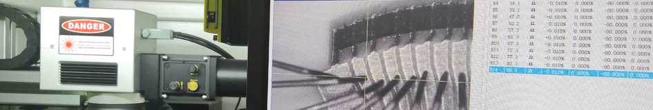
Laser Trimming of Thick Film Hybrid Circuits : |
 |
Laser trimming is a process used in the production of Thick Film Hybrid Circuits to precisely adjust the resistance values of resistors. In the manufacturing process, resistors are screen-printed onto the ceramic substrate along with other electrical traces. However, these resistors may have a tolerance of around +/-20% using the normal production method. To achieve more accurate resistance values, laser trimming is employed. Each resistor is probed and measured for its actual resistance. If the measured resistance is below the target or nominal value, a laser selectively removes some of the resistive material. By doing so, the area through which current flows is reduced, effectively increasing the resistance value. This allows for tighter control over the resistance values of the resistors, typically achieving tolerances better than +/-1%. Laser trimming helps improve the precision and performance of thick film hybrid circuits by ensuring that the resistors meet the required specifications. |
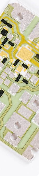
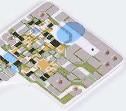
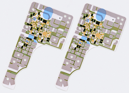
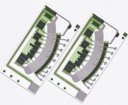
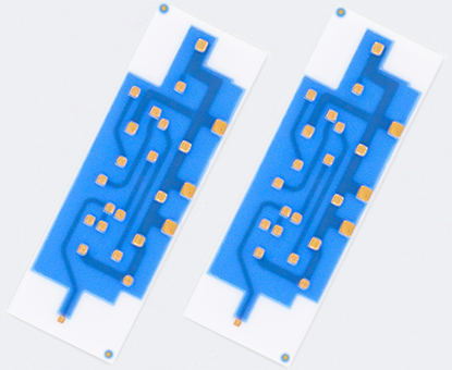
Typical Stack-Up of Thick Film Hybrid Circuits : |
The specific arrangement and number of layers in a Thick Film Hybrid Circuit can vary based on the desired functionality, complexity, and application requirements of the circuit. A typical stack-up of thick film hybrid circuits includes the following layers: 1, Ceramic Substrate: The base layer, made of materials such as alumina (Al2O3), beryllium oxide (BeO), or aluminum nitride (AlN). The substrate provides structural support and serves as a foundation for the circuitry. |
|
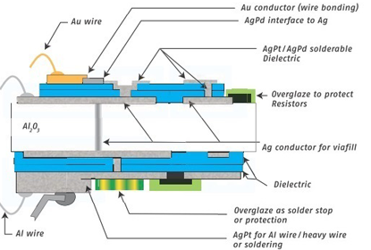 |
2, Conductor Layer: The next layer is the conductor layer, which consists of metallic traces printed onto the ceramic substrate. These metallic traces can be made of materials like silver-palladium, gold-palladium, or other conductive metals. 3, Dielectric Layer: Above the conductor layer, a dielectric layer is applied. This layer provides insulation and serves as a barrier between different circuit elements, preventing short circuits and interference. 4, Resistor Layer: If resistors are incorporated into the circuit design, a resistor layer is added. This layer contains screen-printed resistors that provide specific resistance values in the circuit. 5, Additional Layers: Depending on the circuit design and requirements, additional layers can be added. These may include capacitors, inductors, or other passive components, which are integrated into the stack-up to fulfill specific functions. |
6, Protective Coating: To safeguard the circuitry from external factors like moisture, temperature, and physical damage, a protective coating or solder mask may be applied on top. This layer acts as a barrier and ensures the longevity and reliability of the thick film hybrid circuits. |
|
Why Choose PANDA PCB For Thick Film Hybrid Circuits ? |
At PANDA PCB Group - Thick Film Hybrid Circuits, we specialize in providing Thick Film Solutions that offer exceptional circuit density, high performance, reliability, and cost-effectiveness. With over 20 years of experience, we have established ourselves as experts in the design and manufacture of Thick Film Hybrid Circuits for various industries such as aerospace & defense, automotive, industrial, consumer electronics, healthcare, power generation, and military applications. Here are the top reasons why you should choose Panda PCB: |
|
 |
1, Expertise and Experience: We have been in the industry for over a decade, accumulating extensive knowledge and expertise in manufacturing thick film hybrid circuits. Our team of skilled engineers and technicians ensures the highest quality products and efficient production processes. 2, Customization Options: We understand that every project is unique, and we offer a wide range of customization options to meet your specific requirements. Whether it's different sizes, shapes, or specifications, our team can tailor the thick film hybrid circuits to your exact needs. 3, Quality Assurance: At Panda PCB, quality is our top priority. We adhere to strict quality control measures throughout the manufacturing process to guarantee the reliability and durability of our products. Each thick film hybrid circuit undergoes rigorous testing and inspection before it reaches your hands. |
4, Excellent Customer Support: Our dedicated customer support team is always available to assist you throughout the entire process. From initial inquiries to after-sales support, we are committed to providing excellent service and addressing any concerns or inquiries promptly. |
|
 |
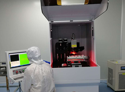
5, State-of-the-Art Facilities: Panda PCB boasts state-of-the-art facilities equipped with advanced machinery and equipment. From design to production, we employ the latest technology to ensure precision, reliability, and excellent performance in our thick film hybrid circuits. 6, Timely Delivery: We understand the importance of meeting deadlines. With our efficient production processes and streamlined logistics, we ensure prompt delivery of your orders. You can rely on us to fulfill your requirements within the agreed-upon timeframe. 7, Competitive Pricing: We believe that premium quality shouldn't come at an exorbitant price. Panda PCB offers competitive pricing without compromising on the quality of our thick film hybrid circuits. We strive to provide cost-effective solutions that meet your budgetary constraints. |
Make the smart choice for your Thick Film Hybrid Circuits. Choose Panda PCB and experience the reliability, quality, and efficiency that sets us apart from the competition. Contact us today to discuss your project and discover how we can fulfill your needs. |
|
Design Guidelines of Thick Film Hybrid Circuits : |
We compiled a Thick Film Hybrid Circuits-Design Guidelines as attached for you to download, It is to better support our customers' needs in designing and applying Thick Film Hybrid Circuits, This guide covers detailed information on product solutions, engineering design specifications, material properties, available manufacturing processes, and more. We hope that this guide will assist customers in standardizing their design process while ensuring the manufacturability of the design data, ultimately improving product reliability and production efficiency. Customers are encouraged to refer to the guide when designing Thick Film Hybrid Circuits to ensure adherence to best practices. |
Capabilities of Thick Film Hybrid Circuits Are As Follows : |
1, Optional Processes of Thick Film Hybrid Circuits :
Metalization Types : |
Thick Film Substrates (Screen-Printed) |
Thin Film Substrates (Photo-Imaged) |
|||
Process Types : |
TFM Capabilities |
HTCC / LTCC Capabilities |
DBC Capabilities |
DPC Capabilities |
AMB Capabilities |
Layer Counts : |
1, 2, 3, 4, 5, 6 Layers |
1, 2, 4, 6, 8, 10, 12 Layers |
1, 2 Layers |
1, 2 Layers |
1, 2 Layers |
Max Board Dimension : |
200*230mm |
200*200mm |
138*178mm |
138*190mm |
114*114mm |
Min Board Thickness : |
0.25mm |
0.25mm |
0.30mm~0.40mm |
0.25mm |
0.25mm |
Max Board Thickness : |
2.2mm |
2.0mm |
1L: 1.6mm; 2L 2.0mm |
2.0mm |
1.8mm |
Conductor Thickness : |
10um - 20um |
5um - 1500um |
1oz - 9oz |
1um - 1000um |
1oz- 22oz |
Min Line Width/Space : |
8/8mil (0.20/0.20mm) |
6/6mil (0.15/0.15mm) |
10/10mil (0.25/0.25mm) |
6/6mil (0.15/0.15mm) |
12/12mil (0.30/0.30mm) |
Substrates Types : |
AI203, ALN, BeO, ZrO2 |
AI203, ALN, BeO, ZrO2 |
Al2O3, AlN, ZrO2, PbO, SiO2, ZTA, Si3N4, SiC, Sapphire, Polycrystalline Silicon, Piezoelectric Ceramics |
Al2O3, AlN, ZrO2, PbO, SiO2, ZTA, Si3N4, SiC, Sapphire, Polycrystalline Silicon, Piezoelectric Ceramics |
AI203, ALN, BeO, ZrO2, Si3N4 |
Min Hole Diameter : |
4mil (0.15mm) |
4mil (0.15mm) |
4mil (0.1mm) |
4mil (0.1mm) |
4mil (0.1mm) |
Outline Tolerance : |
Laser: +/-0.05mm; Die Punch: +/-0.10mm |
Laser: +/-0.05mm; Die Punch: +/-0.10mm |
Laser: +/-0.05mm; Die Punch: +/-0.10mm |
Laser: +/-0.05mm; Die Punch: +/-0.10mm |
Laser: +/-0.05mm; Die Punch: +/-0.10mm |
Substrate Thickness : |
0.25, 0.38, 0.50, 0.635, 0.80,1.0, 1.25, 1.5, 2.0mm, Customizable |
0.25, 0.38, 0.50, 0.635, 0.80,1.0, 1.25, 1.5, 2.0mm, Customizable |
0.25, 0.38, 0.50, 0.635, 0.80,1.0, 1.25, 1.5, 2.0mm, Customizable |
0.25, 0.38, 0.50, 0.635, 0.80,1.0, 1.25, 1.5, 2.0mm, Customizable |
0.25, 0.38, 0.50, 0.635, 0.80,1.0, 1.25, 1.5, 2.0mm, Customizable |
Thickness Tolerance : |
0.25-0.38: +/-0.03mm; 0.50-2.00: +/-0.05mm |
0.25-0.38: +/-0.03mm; 0.50-2.00: +/-0.05mm |
0.25-0.38: +/-0.03mm; 0.50-2.00: +/-0.05mm |
0.25-0.38: +/-0.03mm; 0.50-2.00: +/-0.05mm |
0.25-0.38: +/-0.03mm; 0.50-2.00: +/-0.05mm |
Surface Treatment : |
Ag, Au, AgPd, AuPd |
Ag, Au, AgPd, AuPd, Mn/Ni |
OSP/Ni Plating, ENIG |
OSP/ENIG/ENEPIG |
OSP/ENIG/ENEPIG |
Min Solder PAD Dia : |
10mil (0.25mm) |
10mil (0.25mm) |
8mil (0.20mm) |
6mil (0.15mm) |
8mil (0.20mm) |
2, Engineering Specification of Thick Film Hybrid Circuits :
Items : |
Typical Values |
Advanced Capabilities |
1, Substrates : |
FR4, Ceramic ( AI203, ALN, BeO, ZrO2), Polyimide (Flexible PI), Stainless Steel (SUS304), Mica |
FR4, Ceramic ( AI203, ALN, BeO, ZrO2), Polyimide (Flexible PI), Stainless Steel (SUS304), Mica |
2, Conductor (Paste) Materials : |
Copper, Silver , Gold , Silver-Palladium, Palladium-Gold, Platinum-Silver, Platinum-Gold |
Copper, Silver , Gold , Silver-Palladium, Palladium-Gold, Platinum-Silver, Platinum-Gold |
3, Thick Film Carbon Thickness (Height) : |
15um +/-5 um |
30um +/-5 um |
4, Conductor Thickness (Height) : |
12um+/-5um |
20um+/-5um |
5, Min Width of Thick Film Line : |
0.30 mm +/-0.05 mm |
0.20 mm +/-0.05 mm |
6, Min Space of Thick Film Line : |
0.30 mm +/-0.05 mm |
0.20 mm +/-0.05 mm |
7, Min Overlap (Carbon to Conductor) : |
No less than 0.25mm |
0.20mm (Minimum) |
8, Sheet Resistivity (ohms/square): |
Printed resistors in milli ohm to mega ohm range (Customizable) with tolerances of 1-10% are fabricated and protected with overglaze materials. |
Printed resistors in milli ohm to mega ohm range (Customizable) with tolerances of 0.5-10% are fabricated and protected with overglaze materials. |
9, Resistor Value Tolerance (ohms) : |
+/-10.0% (Standard) (Customizable) |
+/-0.5% (Laser trimming) |
10, Linearity : |
+/-1.0% (Standard) (Customizable) |
+/-0.2 ~ +/-0.5% (Laser trimming) |
11, Synchronism of Double Channels : |
+/-2.0% (Standard) (Customizable) (Potentiometers) |
+/-1.0% (Laser trimming) (Potentiometers) |
12, Durability of Carbon Ink (Life time) : |
0.5 Million (Min), 2.0 Million (Standard) |
5.0-10.0 Million (Max) with Surface Polishing |
13, Working Temperature : |
- 40ºC /+150ºC |
- 40ºC /+180ºC |
3, Optional Substrates of Thick Film Hybrid Circuits :
Substrates : |
Alumina (Al2O3) |
Aluminum Nitride (AlN) |
Beryllium Oxide (BeO) |
Zirconium Dioxide (ZrO2) |
Max Application Temperature : |
662 - 1832 |
1832 |
2300 |
2432 |
Max Power Density (W/in²): |
75 |
1010 |
250 |
300 |
Max Ramp Up Speed (°F/sec): |
122 |
572 |
400 |
350 |
Thermal Conductivity (W/mK): |
20-35 |
180-220 |
200-300 |
2.0-5.0 |
Density (g/cm³): |
3.75 |
3.26 |
2.8 |
5.9 |
Dielectric Loss: |
0.0001 - 0.001 |
0.0001 - 0.0005 |
0.0001 - 0.0002 |
0.0005 - 0.001 |
Dielectric Constant: |
9.4 - 10.2 |
8.5 - 9.0 |
6.0 - 7.0 |
25 - 30 |
CTE, ppm/ºC: |
6.0 - 8.0 |
4.0 - 5.0 |
7.0 - 9.0 |
10.0 - 11.0 |
Substrate Thickness (mm): |
0.25 - 2.0 |
0.25 - 2.0 |
0.25 - 2.0 |
0.25 - 2.0 |
Typical Max. Dimension (inch): |
6 x 12 |
5 x 11 |
6 x 6 |
4 x 4 |
Theoretical Total Wattage (W): |
5400 |
55000 |
15000 |
20000 |
4, Conductive Paste of Thick Film Hybrid Circuits :
Paste ( Materials) : |
Conductor Width/Space |
Soldering / Bonding |
Gold : |
8/8mil (0.20/0.20mm) |
Gold is a good conductor material and allows thermo-compression gold wire bonding and eutectic die attachment. It is, of course, costly and has poor solderability. |
Silver : |
8/8mil (0.20/0.20mm) |
Soldering & Silver is lower in cost, and solderable, but is not leach-resistant with tin/lead solders.More seriously, silver atoms migrate under the influence of DC electric fields, both causing short-circuits and reacting with many of the resistor paste formulations. |
Platinum-Silver : |
6/6mil (0.15/0.15mm) |
Soldering & Surface Mount, Palladium and platinum alloyed to the gold and silver produce good conductor pastes,with good adhesion to the substrate, good solderability, and moderately good wire bonding characteristics. Copper and nickel are examples of materials that have been proposed for paste systems as substitutes for noble metals. |
Palladium-Silver : |
8/8mil (0.20/0.20mm) |
Soldering & Surface Mount ,Solderable, Wire bondable, (good aged adhesion general purpose), Silver-palladium conductor inks are the most commonly used materials, with both price and performance (primarily resistance to solder) increasing with palladium content. |
Platinum-Gold : |
6/6mil (0.15/0.15mm) |
Soldering & Au or Al Wire Bonding, Solderable (excellent aged adhesion with no migration). |
Palladium-Gold : |
8/8mil (0.20/0.20mm) |
Soldering & Au or Al Wire Bonding, Wire bondable. |
5, Resistive Paste of Thick Film Hybrid Circuits :
Performances : |
Common Values/Range |
Description |
Resistance Value : |
1Ω to several MΩ |
The resistance value depends on the type and ratio of carbon black, typically ranging from 1Ω to Mega ohm. |
Resistance Tolerance : |
±1% to ±10% |
High-precision resistors can achieve ±0.1% tolerance used laser trimming process. |
Temperature Coefficient (TCR) : |
±50ppm/°C to ±200ppm/°C |
High-quality resistive paste should have a low TCR, preferably below ±100ppm/°C. |
Stability : |
≤1% |
Resistors must undergo high-temperature aging and humidity tests to ensure stability. |
Sintering Temperature : |
850°C to 950°C |
The sintering temperature for carbon paste depends on material properties, typically in this range. |
Conductivity : |
10⁶ S/m to 10⁸ S/m |
Conductivity depends on the type and ratio of carbon black, affecting resistance precision and stability. |
Surface Smoothness : |
Ra≤ 1 μm |
The surface must be free of cracks, bubbles, and non-uniform layers to ensure good mechanical and electrical properties. |
Insulation Resistance : |
≥10⁹ Ω |
Carbon paste should have good insulation properties to avoid leakage or short circuits. |
Mechanical Strength : |
≥100 MPa |
The resistive layer must have good compressive and bending strength to ensure the reliability of the resistor. |
Volatility : |
Solvent residue ≤ 1% |
High volatility solvents help with even coating and drying, but excessive volatility may affect electrical performance. |
Oxidation Resistance : |
>1000 hours |
High-quality carbon paste should have strong oxidation resistance to extend the service life. |
Humidity Resistance : |
≥1000 hours |
Resistors should be able to withstand high-humidity conditions to ensure long-term stable performance, no significant changes. |
6, Dielectric Paste of Thick Film Hybrid Circuits :
1, High Dielectric Strength: This characteristic enables the paste to be printed between two conductor layers as an insulating layer for Multilayer-Thick Film Hybrid Circuits, providing reliable electrical insulation and preventing breakdown under high electric fields. 2, Good Insulation Resistance: The paste exhibits excellent insulation resistance when printed and covered on a conductor layer, serving as a protective barrier to prevent current leakage and ensuring the integrity of the circuit. 3, Low Power Factor: When applied on a metal core (Stainless steel), the paste serves as an insulating layer for thick film heating elements, demonstrating low power loss and efficient heat generation without compromising electrical insulation. 4, High Dielectric Constant for Thick Film Resistor Elements: The paste is advantageous for fabricating thick film resistor elements, as a high dielectric constant contributes to stability. A dielectric constant of around 10 is optimal for stability, as materials with higher K values may exhibit thermal coefficient issues, impacting performance in applications requiring stability. |
7, Insulating Paste of Thick Film Hybrid Circuits :
Commonly used non-metallic materials for protective coatings include overglazes (Glass-Glaze), enamel, polymers, and epoxies,depending on application conditions and environment with several intents: mechanically protecting physical damage, electrically insulating the heating traces, preventing corrosion along with water resistance, thermally withstanding maximum application temperatures, against outgassing in high vacuum (Vacuum protection), and withstand high voltage. 1, Dielectric Strength: The dielectric strength of the insulating paste indicates its ability to withstand electric fields without breaking down, and it is a crucial specification for ensuring the reliability of the thick film hybrid circuit. 2, Insulation Resistance: This specification measures the resistance of the insulating paste to electric current flow through it. High insulation resistance is essential for preventing leakage currents and maintaining the integrity of the circuit. 3, Thermal Conductivity: The thermal conductivity of the insulating paste affects its ability to dissipate heat from components and substrates in the circuit. This parameter is important for managing temperature and ensuring proper performance. 4, Thermal Stability: The ability of the insulating paste to maintain its properties and integrity at elevated temperatures is critical for long-term reliability in high-temperature applications. 5, Adhesion Strength: Specifications related to the adhesion strength of the insulating paste to substrate materials can ensure proper bonding and prevent delamination or detachment during operation or manufacturing processes. 6, Compatibility: Compatibility with other materials used in thick film hybrid circuits, such as conductor pastes and resistive pastes, should be outlined to ensure proper integration and performance. |