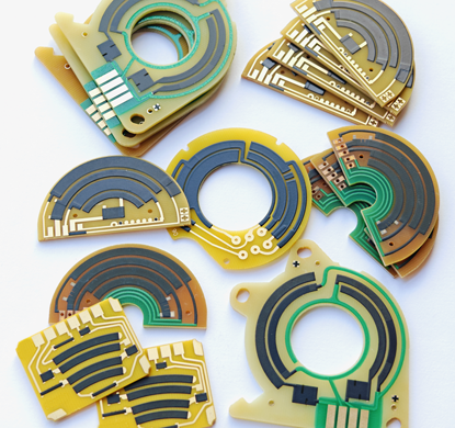
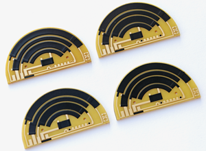
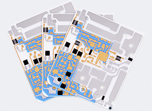
Thick Film Technology
Thick Film Technologies, also known as Thick Film Solutions, are highly reliable manufacturing technologies widely used in the production of hybrid integrated circuits and semiconductor components, with the main fabrication processes involving applying conductive, resistive, dielectric, and insulating materials onto substrates such as PI, FR4, ceramics, or glass, followed by curing, high-temperature sintering, and laser trimming, which results in high-precision, diverse, and customizable thick-film hybrid integrated electronic circuits with excellent cost-effectiveness. Thick Film Technologies are known for their high durability, versatility, and reliability. The materials used offer excellent electrical conductivity, thermal resistance, and stability, making them ideal for harsh environments. These technologies support high integration, allowing resistors, capacitors, and other components to be directly applied to substrates. Additionally, they can be customized to meet specific performance requirements, offering design flexibility while keeping manufacturing costs low. Thick Film Solutions are widely used across industries such as automotive, telecommunications, consumer electronics, and medical devices. In automotive applications, they are found in engine control systems, sensors, and power modules, requiring high reliability and resistance to extreme temperatures. In telecommunications, they are integral to signal processing and network equipment. These technologies also play a key role in medical devices, where precision and high performance are critical. Their ability to integrate multiple functions into compact, reliable, and cost-effective components makes them essential in these fields, driving advancements in electronics and semiconductors. Process Features of Thick Film Technology : |
 |
|
 |
1, Substrate Preparation: The process begins with preparing the substrate, which is typically made of materials such as FR4, Alumina (Ceramic), Polyester, Polyimide (Flexible PCB), Stainless Steel (SUS304), Mica, and Metal Core. The substrate surface is meticulously cleaned and treated to ensure optimal adhesion of the thick film materials. 2, Thick Film Paste Preparation: The thick film paste used to create thick film circuits is broadly categorized into three types: Dielectric paste, Conductive paste, and Resistive paste. Dielectric paste is generally glass and ceramic-based and non-conductive. Conductive paste contains precious metal particles such as Silver, Gold, Silver-Palladium, Gold-Platinum, and their alloys. Resistive paste comprises blends of glasses, metals, and metal oxides, such as silver and ruthenium, in various combinations to achieve inks with different resistance values. |
|
3, Thick Film Printing: The printing of thick film materials, including conductive pastes, resistive pastes, and dielectric pastes, onto the substrate is accomplished using various methods. Common techniques include screen printing, stencil printing, and inkjet printing. 4, Drying and Firing Process: Following the coating of thick film materials, the substrate undergoes a drying process to eliminate any solvents or moisture from the film. Subsequently, the substrate is fired in a high-temperature furnace to sinter and bond the thick film materials to the substrate. This involves pre-drying in an oven at 200°C before being baked at around 850°C. The firing temperature and time are precisely controlled to achieve the desired electrical and mechanical properties. |
||
 |
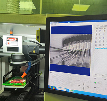
5, Metallization Process: Thick Film Technology utilizes various metals to barrel coat and plug holes drilled through the ceramic substrate. When incorporating metallized through holes in a design, the opposite side of the board can serve as a separated or connected circuit. PTH with metallization connections can be used to integrate various other conductor layers, providing a significant advantage when high circuit density is required. 6, Laser Trimming Process: Screen printed resistors produced by the normal process typically have a value tolerance of about +/-20%. Laser trimming can be employed to reduce variability to better than +/-1%. In laser trimming, each resistor is probed to measure its actual resistance. If it is below the nominal or target value, a laser selectively removes resistive material to reduce the area through which current flows, thereby increasing the resistance. 7, Post-Processing: Additional processes may be performed, as needed, once the thick film circuit or component is formed. These processes can include trimming, laser machining, encapsulation, and surface finishing to enhance the performance, durability, and aesthetics of the product. |
|
Key Advantages of Thick Film Technology : |
Thick Film Technology offers several key advantages that make it a popular choice in a wide range of electronic applications, especially in industries like automotive, telecommunications, power electronics, and consumer electronics. 1. Cost-Effective Production : ● Scalability: Thick Film Technology is suitable for mass production, and its processes (like screen printing) can be easily scaled to produce large quantities of components quickly and efficiently. This is ideal for applications that require cost-effective, high-volume manufacturing. 2. High Reliability : ● Stable Performance: Thick Film Technology offers stable electrical properties over a wide range of temperatures and environmental conditions. This ensures reliable performance over time, even in harsh environments. |
|
 |
3. Versatility in Material Choices : ● High-Performance Materials: Conductive materials like silver, gold, and palladium are commonly used, providing excellent electrical conductivity. Metal oxide materials used for resistive layers offer stability and precision for a wide range of resistances. 4. Ability to Handle High Power : ● Improved Heat Dissipation: The thicker film layers allow for better heat dissipation, which is crucial in high-power applications. This helps in maintaining the reliability and performance of devices under high-temperature conditions. |
5. Robustness and Durability : ● Chemical Stability: Thick film components are also resistant to corrosion and oxidation, which makes them ideal for use in environments that expose them to chemicals or humidity. 6. Miniaturization and Integration : ● Multilayer Integration: Thick Film Technology can be used to create multilayer circuits, allowing for higher component density on the same substrate. This increases functionality while reducing the overall size of the final device. |
|
 |
7. Compatibility with Diverse Substrates : ● Substrate Customization: Substrates can be tailored for specific applications. For example, ceramic substrates can be selected for their high thermal resistance, while glass substrates can be chosen for their transparency in certain optical applications. 8. Environmental and Sustainability Benefits : ● Reduced Energy Consumption: The manufacturing process for Thick Film Technology, particularly in terms of materials coating (such as screen printing), generally consumes less energy compared to other methods like thin film deposition, contributing to a lower environmental impact. |
9. Customization and Design Flexibility : ● Prototyping and Small-Batch Production: Thick Film Technology is well-suited for prototyping and small-batch production. Designers can quickly iterate on new designs without significant investment in tooling or specialized equipment. 10. Excellent Electrical Performance : ● Low Parasitic Effects: Since thick film components can be made directly onto substrates, there are fewer parasitic effects (such as inductance and capacitance) compared to traditional wire-bonded or leaded components. Thick Film Technologies are valued for their cost-effectiveness, high power handling, reliability, and versatility in both materials and applications. These advantages make them a preferred choice for mass production of components that need to operate under harsh conditions, such as automotive electronics, power devices, sensors, and industrial applications. The ability to integrate multiple components onto a single substrate, along with excellent electrical performance and robustness, further strengthens their appeal in diverse electronic applications. |
|
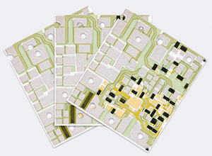
Typical Solutions Offered by Thick Film Technology : |
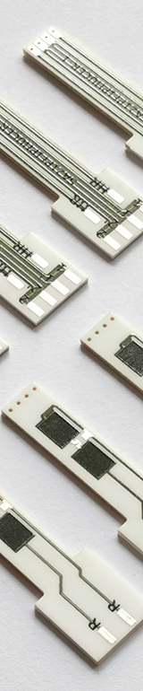
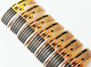
Thick Film Technologies offer a range of solutions, including hybrid circuits, ceramic PCBs, heaters, resistors, and sensor systems. Products made with Thick Film Technologies feature excellent thermal conductivity, resistance to extreme temperatures and chemicals, and are suitable for mass production. These solutions are widely used in industries such as automotive, telecommunications, and medical devices, providing reliable and customizable components. 1, Thick Film Resistor PCBs are highly efficient and unique printed circuit boards that allow designers to selectively integrate resistive, capacitive sensors, or heating elements into electronic circuits, using thick-film technology to print conductive, resistive, and insulating materials to PI, FR4, or ceramic PCBs, followed by high-temperature curing, sintering, photolithography, and laser trimming processes, which form precise and reliable thick film hybrid circuits that provide customized solutions for various electronic systems. |
|
 |
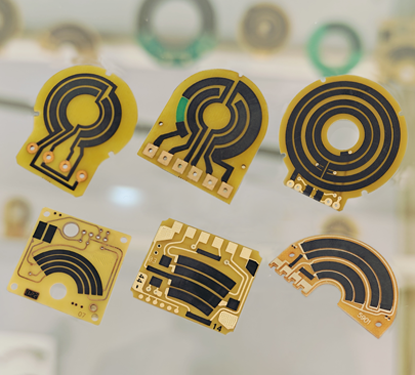
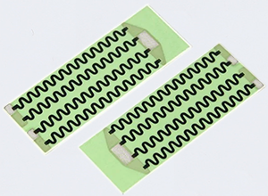
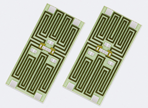
2, Thick Film Circuits offer versatility and reliability by integrating conductive, resistive, and insulating materials on a single ceramic substrate. They are highly resistant to high temperatures, humidity, and mechanical stress, making them ideal for harsh environments. Cost-effective by reducing wiring and assembly needs, these circuits lower production costs while ensuring precise and durable components. 3, Thick Film Ceramic PCBs are built with ceramic substrates like alumina (aluminum oxide) or aluminum nitride, which offer superior thermal conductivity, mechanical strength, and chemical resistance compared to the traditional fiberglass epoxy (FR4) substrate found in standard PCBs. These ceramic materials make the PCBs highly suitable for applications in environments that demand high thermal management and resistance to harsh chemicals, mechanical stresses, and extreme temperatures. 4, Thick Film Heaters generate heat by passing an electric current through a resistive layer, utilizing the resistive heating effect to convert electrical energy into heat. The uniform thickness and stable materials of the resistive layer ensure even heat distribution, maintaining consistent heating performance. Additionally, thick film technology allows for precise customization of the heating areas, enabling adjustments to power and shape based on specific application requirements, thus providing accurate temperature control. |
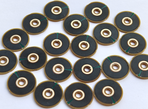
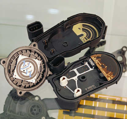
5, Thick Film Ceramic Resistors are precision electronic components designed to control the flow of current in a circuit, serving functions such as circuit regulation, power distribution, and protection, and are manufactured using thick film technology where resistive and conductive materials are printed onto a ceramic substrate, followed by high-temperature sintering and laser trimming to form a stable, durable, reliable, and customizable resistor element on the surface of the ceramic substrate. 6, Thick Film Sensors operate based on the principle of resistance change. The thick film material applied to the sensor's surface undergoes physical property changes in response to environmental factors such as temperature, pressure, or humidity, resulting in variations in resistance. For example, when external pressure changes, the thick film material inside the sensor may deform or compress, leading to a corresponding change in resistance. The sensor's circuit system continuously monitors these changes and outputs signals that reflect the changes in environmental parameters. |
|
Product Types of Thick Film Technology : |
Applications of Thick Film Solutions : |
Thick Film Solutions are commonly used in various industries due to their versatile properties and cost-effectiveness. These solutions typically consist of a mix of conductive and non-conductive materials, applied to a substrate to create electronic circuits, sensors, and other components. Below are the primary applications of thick film solutions: 1, Electronics Manufacturing: Thick film solutions are predominantly used in the production of resistors, capacitors, inductors, and hybrid integrated circuits. The films are applied to ceramic substrates, where they form the basis for passive components that are essential in electronic devices such as mobile phones, computers, and automotive electronics. |
|
 |
2, Sensor Technology: Thick film technology is widely used in the creation of sensors, including temperature sensors, gas sensors, and pressure sensors. The films provide a robust and reliable method for detecting and converting physical phenomena into electrical signals. 3, Hybrid Circuits: Thick film solutions offer a way to create complex circuits on ceramic or FR4 substrates. These circuits combine active elements like semiconductors with passive components to form a complete functional system. 4, Power Electronics: Thick film materials are ideal for applications in power electronics, where high reliability and resistance to environmental stresses are required. This includes power resistors, high-voltage components, and power distribution systems. 5, Automotive Industry: Thick film solutions are used in automotive applications for components like ignition systems, electronic control units (ECUs), and sensors. The ability to withstand high temperatures and harsh conditions makes them suitable for automotive electronics. |
6, Displays and Imaging: Thick film technology plays a role in display applications such as flat-panel displays, touchscreens, and image sensors. The films are used to create transparent conductive layers or electrode patterns. 7, Microwave and RF Applications: Due to their stability and resistance to environmental factors, thick films are employed in microwave and radio-frequency (RF) devices, including antennas, filters, and waveguides. 8, Solar Energy: In the solar energy sector, thick film solutions are applied in the production of photovoltaic cells and panels. The films contribute to efficient energy conversion and are used in various types of solar cells for both residential and industrial applications. These applications highlight the broad and growing utility of thick film solutions in a range of industries, driven by their ability to provide precise and durable circuit patterns, cost-effectiveness, and adaptability to a variety of environments. |
|
The Most Representative Applications of Thick Film Solutions : |
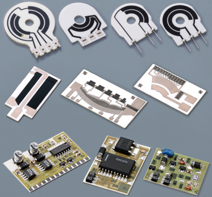
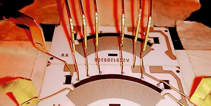
1, Linear potentiometers , Rotary potentiometers. |
1, High voltage ceramic resistor. |
1, Storage room heaters. |
Typical Applications of Thick Film Solutions in Automotive Electronics : |
Thick Film Solutions find various applications in automotive electronics due to its versatility, reliability, and cost-effectiveness. Here are some specific applications of thick film technology in the automotive industry: 1, Power Modules: Thick film solutions are employed in the manufacturing of power modules used in electric and hybrid vehicles. These modules incorporate thick film resistors, capacitors, and conductive traces to manage and distribute electrical power within the vehicle's propulsion and energy storage systems. |
|
 |
2, Throttle Position Sensor: Thick film solutions are employed in the production of throttle position sensors used in electronic throttle control systems. These sensors utilize resistive thick film materials to detect the position of the throttle valve, providing crucial input to the engine management system for precise fuel injection and power delivery. 3, Ignition Module: Thick film solutions are utilized in the manufacturing of ignition modules, particularly in the construction of ignition control units and ignition coil drivers. This technology enables the integration of resistors, capacitors, and conductive traces within the ignition module, contributing to reliable ignition timing and spark control. 4, Voltage Regulator: Thick film resistors are commonly used in voltage regulator modules within the vehicle's electrical system. These resistors play a key role in regulating voltage levels for various automotive electrical components, ensuring stable and consistent power supply under varying operating conditions. 5, Fuel Level Sensor: Thick film solutions are applied in the development of fuel level sensors used to measure the quantity of fuel in the vehicle's tank. By utilizing resistive thick film materials, these sensors provide accurate readings to the fuel gauge and onboard computer systems, allowing drivers to monitor fuel levels accurately. |
6, Accelerator Pedal Position Sensor: A key application of Thick Film Solutions in automotive electronics, the Accelerator Pedal Position Sensor (APPS) detects the actual position of the driver’s accelerator pedal and sends this data to the Engine Control Unit (ECU). The ECU then adjusts engine power output and throttle response accordingly. The integration of Thick Film Solutions technology in APPS ensures high precision, reliability, and durability, meeting the stringent performance requirements of modern automotive sensors. 7, Heating Elements: Thick film solutions are applied to produce heating elements used in automotive applications such as seat heaters, heated mirrors, windshield defrosters, and diesel fuel heaters. These heating elements offer efficient and even heat distribution while withstanding the harsh conditions. 8, Displays and Instrumentation: Thick film solutions are used to create thin, robust, and customizable display panels for automotive instrument clusters, infotainment systems, and dashboard displays. The technology enables the production of high-resolution and durable displays suitable for automotive environments. 9, EV and HEV (Electric Vehicle and Hybrid Electric Vehicle): Thick film solutions can meet the electrical requirements of EV and HEV power modules. such as power modules for electric vehicles and hybrid electric vehicles, call for higher voltage and power from smaller circuits, requiring circuit materials capable of providing high voltage isolation with the efficient dissipation of heat from densely packed semiconductor devices. In each of these applications, Thick Film Solutions offer benefits such as compact design, precise electrical characteristics, and the ability to withstand harsh automotive environments, making it an ideal choice for automotive electronic components. |
|
Laser Trimming of Thick Film Technology : |
 |
● Laser trimming is a technique commonly used in thick film technology to precisely adjust the resistance values of resistors. In the manufacturing process of thick film circuits, resistors are screen-printed onto the ceramic substrate along with other conductive traces and components, Laser trimming is an essential technique utilized in thick film technology to ensure the accuracy and reliability of resistors and enhance the overall functionality of thick film hybrid circuits. ● However, due to variations in materials and printing processes, the resistors may have slight deviations from their intended resistance values. Laser trimming is employed to fine-tune these resistors to meet the desired specifications. |
● During laser trimming, each resistor is probed and its actual resistance is measured. If the resistance is found to be too high or too low compared to the target value, a high-precision laser is used to selectively remove or ablate a small amount of the resistive material. By adjusting the dimensions of the resistor, the laser trimming process finely tunes the resistance to the desired value. ● Laser trimming offers several advantages in the production of thick film hybrid circuits. It enables precise resistance adjustment, allowing for tighter tolerance control and improved circuit performance. Additionally, laser trimming eliminates the need for using numerous resistor values and provides flexibility in achieving specific resistance values within a circuit design. |
|
Typical Stack-Up of Multilayer-Thick Film Substrates : |
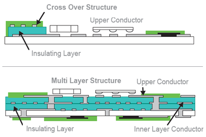 |
A stack-up of Multilayer-Thick Film Substrates based on thick film technology typically involves the following layers: 2, Conductive Layers: Multiple conductor layers are incorporated into the stack-up. These layers consist of metallic traces, typically made of materials like silver-palladium, gold-palladium, or other conductive metals. Each conductor layer contributes to the overall circuit connectivity. 3, Dielectric Layers: In between the conductor layers, dielectric layers are added for insulation. These layers provide electrical isolation between the different conductive layers, preventing signal interference and short circuits. |
4, Vias: Vias are small openings that traverse through the dielectric layers, connecting the different conductor layers. They allow electrical signals to pass between the various layers and provide interlayer connectivity. 5, Plated Through-Holes (PTH): PTH refers to vias that extend through the entire stack-up, from the top to the bottom surface of the circuit. These through-holes are plated or filled with a conductive material, ensuring electrical continuity between the layers. By the way, Hole size greater than 0.45mm is not recommended. 6, Additional Layers: Depending on the complexity and functionality requirements of the circuit design, additional layers can be included. These may involve components such as capacitors, inductors, or resistors, which are integrated within the stack-up. 7, Solder Mask or Overglazes: A protective solder mask is applied on top of the circuit layers. This coating helps protect the circuit from moisture, temperature, and physical damage, ensuring its reliability and longevity. |
|
Design Considerations of Thick Film Technology : |
Thick Film Technologies require careful consideration of several factors in their designs to ensure the reliability, performance, and cost-effectiveness of the final products. 1. Material Selection : ● Resistive Materials: Metal oxides (e.g., ruthenium oxide, tin oxide) are typically used for resistors. Their resistivity can be adjusted by altering the composition, which is crucial for meeting specific resistance values. ● Insulating Materials: Glass frits and ceramics are used as dielectrics and insulating materials. They must have high dielectric strength and thermal stability to withstand operational conditions. 2. Layer Thickness : ● Uniformity: Achieving uniform thickness across the substrate is crucial for consistent electrical performance. Inconsistent layer thickness can lead to defects, such as short circuits or poor electrical contacts. |
|
 |
3. Substrate Material : ● Thermal Expansion: The coefficient of thermal expansion (CTE) of the substrate should match that of the thick film materials to avoid stresses or cracking due to temperature changes. 4. Circuit Design and Layout : ● Electromagnetic Interference: Circuit layout should minimize interference by optimizing the placement of components like resistors, capacitors, and conductors. The layout should also ensure that signal paths are as short and direct as possible to reduce parasitic inductance and capacitance. |
● Multilayer Integration: Designing a multilayer structure requires careful planning of the sequence in which layers are printed and fired. Each layer must be registered accurately to ensure proper alignment. 5. Firing and Sintering Conditions : ● Firing Atmosphere: The firing atmosphere (oxidizing or reducing) can influence the characteristics of the materials, especially the conductive and resistive layers. The atmosphere should be chosen based on the material composition and desired electrical properties. 6. Power Handling and Heat Dissipation : ● Thermal Management: Ensure that heat is efficiently dissipated from high-power components. This may involve designing for good thermal conductivity in the substrate and ensuring that the components are spaced appropriately. |
|
 |
● Thermal Management: Ensure that heat is efficiently dissipated from high-power components. This may involve designing for good thermal conductivity in the substrate and ensuring that the components are spaced appropriately. 7. Cost and Scalability : ● Manufacturing Scalability: Thick Film Technology is often used in high-volume manufacturing due to its cost efficiency. The design should consider how well the process can be scaled, ensuring consistency and reliability in mass production. 8. Reliability and Testing : ● Electrical Testing: After fabrication, components should undergo rigorous testing (e.g., resistance, capacitance, continuity tests) to ensure the design specifications. |
9. Environmental Considerations : ● Corrosion Resistance: Materials used in the thick film must be resistant to corrosion over time, especially in outdoor or harsh industrial environments. 10. Tolerance and Precision : ● Component Tolerances: The thick film process has inherent tolerances in terms of resistance values and physical dimensions. These tolerances should be specified during the design phase to ensure that the final product meets electrical and functional requirements. Designing for Thick Film Substrates require a comprehensive approach that considers material selection, layer thickness, substrate compatibility, circuit layout, firing conditions, and environmental factors. The goal is to balance performance, durability, and cost while ensuring reliable and scalable production for the intended application. |
|
Why Choose PANDA PCB For Thick Film Solutions ? |
PANDA PCB Group is a leading manufacturer of Thick Film Solutions with over 20 years of experience in the design and fabrication, and there are several reasons why we are an excellent choice for this technology. ● Panda PCB has many years of experience in the field of thick film circuits. Our team of engineers possesses extensive knowledge and expertise in designing and manufacturing these circuits, ensuring that our products are of the highest quality. ● Panda PCB is committed to providing high-quality products to their customers. We use the best materials and follow strict quality control processes to ensure that each thick film hybrid circuit meets or exceeds industry standards. This dedication to quality translates into durable and reliable products that are built to last. |
|
 |
● Panda PCB offers customization options to meet the specific needs of their clients. We understand that each application may have unique requirements, and we are willing to work with our customers to develop a custom thick film resistor PCB solution that fits their needs. ● Panda PCB is a reputable and reliable provider of thick film solutions. Our expertise, focus on quality, customization options, advanced manufacturing facilities, and commitment to customer satisfaction make them an excellent choice for anyone in need of thick film circuits, thick film resistors and thick film heaters. ● Our standard thick film substrate materials include FR4, Flexible PI, Ceramic, Mica and Metal Core. Thick Film Solutions are the method for production of resistive electronic, which have four main applications including Thick Film Resistor PCB, Thick Film Ceramic Resistor, Thick Film Hybrid Circuits, and Thick Film Heaters. |
Design Guidelines of Thick Film Technology : |
We compiled a Thick Film Technology-Design Guidelines as attached for you to download, It is to better support our customers' needs in designing and applying Thick Film Technologies, This guide covers detailed information on product solutions, engineering design specifications, material properties, available manufacturing processes, and more. We hope that this guide will assist customers in standardizing their design process while ensuring the manufacturability of the design data, ultimately improving product reliability and production efficiency. Customers are encouraged to refer to the guide when designing Thick Film Technologies to ensure adherence to best practices. |
Capabilities of Thick Film Technology Are As Follows : |
1, Engineering Specification of Thick Film Technology :
Items : |
Typical Values |
Advanced Capabilities |
1, Substrates : |
FR4, Ceramic ( AI203, ALN, BeO, ZrO2), Polyimide (Flexible PI), Stainless Steel (SUS304), Mica |
FR4, Ceramic ( AI203, ALN, BeO, ZrO2), Polyimide (Flexible PI), Stainless Steel (SUS304), Mica |
2, Conductor (Paste) Materials : |
Copper, Silver , Gold , Silver-Palladium, Palladium-Gold, Platinum-Silver, Platinum-Gold |
Copper, Silver , Gold , Silver-Palladium, Palladium-Gold, Platinum-Silver, Platinum-Gold |
3, Thick Film Carbon Thickness (Height) : |
15um +/-5 um |
30um +/-5 um |
4, Conductor Thickness (Height) : |
12um+/-5um |
20um+/-5um |
5, Min Width of Thick Film Line : |
0.30 mm +/-0.05 mm |
0.20 mm +/-0.05 mm |
6, Min Space of Thick Film Line : |
0.30 mm +/-0.05 mm |
0.20 mm +/-0.05 mm |
7, Min Overlap (Carbon to Conductor) : |
No less than 0.25mm |
0.20mm (Minimum) |
8, Sheet Resistivity (ohms/square): |
Printed resistors in milli ohm to mega ohm range (Customizable) with tolerances of 1-10% are fabricated and protected with overglaze materials. |
Printed resistors in milli ohm to mega ohm range (Customizable) with tolerances of 0.5-10% are fabricated and protected with overglaze materials. |
9, Resistor Value Tolerance (ohms) : |
+/-10.0% (Standard) (Customizable) |
+/-0.5% (Laser trimming) |
10, Linearity : |
+/-1.0% (Standard) (Customizable) |
+/-0.2 ~ +/-0.5% (Laser trimming) |
11, Synchronism of Double Channels : |
+/-2.0% (Standard) (Customizable) (Potentiometers) |
+/-1.0% (Laser trimming) (Potentiometers) |
12, Durability of Carbon Ink (Life time) : |
0.5 Million (Min), 2.0 Million (Standard) |
5.0-10.0 Million (Max) with Surface Polishing |
13, Working Temperature : |
- 40ºC /+150ºC |
- 40ºC /+180ºC |
2, Optional Processes of Thick Film Technology :
Metalization Types : |
Thick Film Substrates (Screen-Printed) |
Thin Film Substrates (Photo-Imaged) |
|||
Process Types : |
TFM Capabilities |
HTCC / LTCC Capabilities |
DBC Capabilities |
DPC Capabilities |
AMB Capabilities |
Layer Counts : |
1, 2, 3, 4, 5, 6 Layers |
1, 2, 4, 6, 8, 10, 12 Layers |
1, 2 Layers |
1, 2 Layers |
1, 2 Layers |
Max Board Dimension : |
200*230mm |
200*200mm |
138*178mm |
138*190mm |
114*114mm |
Min Board Thickness : |
0.25mm |
0.25mm |
0.30mm~0.40mm |
0.25mm |
0.25mm |
Max Board Thickness : |
2.2mm |
2.0mm |
1L: 1.6mm; 2L 2.0mm |
2.0mm |
1.8mm |
Conductor Thickness : |
10um - 20um |
5um - 1500um |
1oz - 9oz |
1um - 1000um |
1oz- 22oz |
Min Line Width/Space : |
8/8mil (0.20/0.20mm) |
6/6mil (0.15/0.15mm) |
10/10mil (0.25/0.25mm) |
6/6mil (0.15/0.15mm) |
12/12mil (0.30/0.30mm) |
Substrates Types : |
AI203, ALN, BeO, ZrO2 |
AI203, ALN, BeO, ZrO2 |
Al2O3, AlN, ZrO2, PbO, SiO2, ZTA, Si3N4, SiC, Sapphire, Polycrystalline Silicon, Piezoelectric Ceramics |
Al2O3, AlN, ZrO2, PbO, SiO2, ZTA, Si3N4, SiC, Sapphire, Polycrystalline Silicon, Piezoelectric Ceramics |
AI203, ALN, BeO, ZrO2, Si3N4 |
Min Hole Diameter : |
4mil (0.15mm) |
4mil (0.15mm) |
4mil (0.1mm) |
4mil (0.1mm) |
4mil (0.1mm) |
Outline Tolerance : |
Laser: +/-0.05mm; Die Punch: +/-0.10mm |
Laser: +/-0.05mm; Die Punch: +/-0.10mm |
Laser: +/-0.05mm; Die Punch: +/-0.10mm |
Laser: +/-0.05mm; Die Punch: +/-0.10mm |
Laser: +/-0.05mm; Die Punch: +/-0.10mm |
Substrate Thickness : |
0.25, 0.38, 0.50, 0.635, 0.80,1.0, 1.25, 1.5, 2.0mm, Customizable |
0.25, 0.38, 0.50, 0.635, 0.80,1.0, 1.25, 1.5, 2.0mm, Customizable |
0.25, 0.38, 0.50, 0.635, 0.80,1.0, 1.25, 1.5, 2.0mm, Customizable |
0.25, 0.38, 0.50, 0.635, 0.80,1.0, 1.25, 1.5, 2.0mm, Customizable |
0.25, 0.38, 0.50, 0.635, 0.80,1.0, 1.25, 1.5, 2.0mm, Customizable |
Thickness Tolerance : |
0.25-0.38: +/-0.03mm; 0.50-2.00: +/-0.05mm |
0.25-0.38: +/-0.03mm; 0.50-2.00: +/-0.05mm |
0.25-0.38: +/-0.03mm; 0.50-2.00: +/-0.05mm |
0.25-0.38: +/-0.03mm; 0.50-2.00: +/-0.05mm |
0.25-0.38: +/-0.03mm; 0.50-2.00: +/-0.05mm |
Surface Treatment : |
Ag, Au, AgPd, AuPd |
Ag, Au, AgPd, AuPd, Mn/Ni |
OSP/Ni Plating, ENIG |
OSP/ENIG/ENEPIG |
OSP/ENIG/ENEPIG |
Min Solder PAD Dia : |
10mil (0.25mm) |
10mil (0.25mm) |
8mil (0.20mm) |
6mil (0.15mm) |
8mil (0.20mm) |
3, Optional Substrates of Thick Film Technology :
Substrates : |
Alumina (Al2O3) |
Aluminum Nitride (AlN) |
Beryllium Oxide (BeO) |
Zirconium Dioxide (ZrO2) |
Max Application Temperature : |
662 - 1832 |
1832 |
2300 |
2432 |
Max Power Density (W/in²): |
75 |
1010 |
250 |
300 |
Max Ramp Up Speed (°F/sec): |
122 |
572 |
400 |
350 |
Thermal Conductivity (W/mK): |
20-35 |
180-220 |
200-300 |
2.0-5.0 |
Density (g/cm³): |
3.75 |
3.26 |
2.8 |
5.9 |
Dielectric Loss: |
0.0001 - 0.001 |
0.0001 - 0.0005 |
0.0001 - 0.0002 |
0.0005 - 0.001 |
Dielectric Constant: |
9.4 - 10.2 |
8.5 - 9.0 |
6.0 - 7.0 |
25 - 30 |
CTE, ppm/ºC: |
6.0 - 8.0 |
4.0 - 5.0 |
7.0 - 9.0 |
10.0 - 11.0 |
Substrate Thickness (mm): |
0.25 - 2.0 |
0.25 - 2.0 |
0.25 - 2.0 |
0.25 - 2.0 |
Typical Max. Dimension (inch): |
6 x 12 |
5 x 11 |
6 x 6 |
4 x 4 |
Theoretical Total Wattage (W): |
5400 |
55000 |
15000 |
20000 |
4, Conductive Paste of Thick Film Technology :
Paste ( Materials) : |
Conductor Width/Space |
Soldering / Bonding |
Gold : |
8/8mil (0.20/0.20mm) |
Gold is a good conductor material and allows thermo-compression gold wire bonding and eutectic die attachment. It is, of course, costly and has poor solderability. |
Silver : |
8/8mil (0.20/0.20mm) |
Soldering & Silver is lower in cost, and solderable, but is not leach-resistant with tin/lead solders.More seriously, silver atoms migrate under the influence of DC electric fields, both causing short-circuits and reacting with many of the resistor paste formulations. |
Platinum-Silver : |
6/6mil (0.15/0.15mm) |
Soldering & Surface Mount, Palladium and platinum alloyed to the gold and silver produce good conductor pastes,with good adhesion to the substrate, good solderability, and moderately good wire bonding characteristics. Copper and nickel are examples of materials that have been proposed for paste systems as substitutes for noble metals. |
Palladium-Silver : |
8/8mil (0.20/0.20mm) |
Soldering & Surface Mount ,Solderable, Wire bondable, (good aged adhesion general purpose), Silver-palladium conductor inks are the most commonly used materials, with both price and performance (primarily resistance to solder) increasing with palladium content. |
Platinum-Gold : |
6/6mil (0.15/0.15mm) |
Soldering & Au or Al Wire Bonding, Solderable (excellent aged adhesion with no migration). |
Palladium-Gold : |
8/8mil (0.20/0.20mm) |
Soldering & Au or Al Wire Bonding, Wire bondable. |
5, Resistive Paste of Thick Film Technology :
Performances : |
Common Values/Range |
Description |
Resistance Value : |
1Ω to several MΩ |
The resistance value depends on the type and ratio of carbon black, typically ranging from 1Ω to Mega ohm. |
Resistance Tolerance : |
±1% to ±10% |
High-precision resistors can achieve ±0.1% tolerance used laser trimming process. |
Temperature Coefficient (TCR) : |
±50ppm/°C to ±200ppm/°C |
High-quality resistive paste should have a low TCR, preferably below ±100ppm/°C. |
Stability : |
≤1% |
Resistors must undergo high-temperature aging and humidity tests to ensure stability. |
Sintering Temperature : |
850°C to 950°C |
The sintering temperature for carbon paste depends on material properties, typically in this range. |
Conductivity : |
10⁶ S/m to 10⁸ S/m |
Conductivity depends on the type and ratio of carbon black, affecting resistance precision and stability. |
Surface Smoothness : |
Ra≤ 1 μm |
The surface must be free of cracks, bubbles, and non-uniform layers to ensure good mechanical and electrical properties. |
Insulation Resistance : |
≥10⁹ Ω |
Carbon paste should have good insulation properties to avoid leakage or short circuits. |
Mechanical Strength : |
≥100 MPa |
The resistive layer must have good compressive and bending strength to ensure the reliability of the resistor. |
Volatility : |
Solvent residue ≤ 1% |
High volatility solvents help with even coating and drying, but excessive volatility may affect electrical performance. |
Oxidation Resistance : |
>1000 hours |
High-quality carbon paste should have strong oxidation resistance to extend the service life. |
Humidity Resistance : |
≥1000 hours |
Resistors should be able to withstand high-humidity conditions to ensure long-term stable performance, no significant changes. |
6, Dielectric Paste of Thick Film Technology :
Performances : |
Typical Value |
Explanation |
Material Types : |
Epoxy Resin (Epoxy), Polyimide (PI), Polyurethane (PU), Polytetrafluoroethylene (PTFE), etc. |
These resin types are commonly used to manufacture dielectric materials, providing good electrical insulation, thermal stability, and mechanical strength. |
Dielectric Constant (εr) : |
3 ~ 4.5 (Epoxy), 3.0 ~ 3.5 (PI), 2.1 ~ 2.5 (PTFE) |
Epoxy and polyimide are typically used in low-to-medium frequency circuits, while PTFE is preferred for high-frequency applications due to its lower dielectric constant. |
Insulation Resistance : |
≥ 10¹² Ω·cm |
Resin-based materials usually exhibit extremely high insulation resistance, effectively isolating electrical currents and preventing leakage. |
Dielectric Loss : |
≤ 0.01 (Epoxy), ≤ 0.005 (PI), ≤ 0.0002 (PTFE) |
Polyimide and PTFE have lower dielectric loss, making them ideal for high-frequency applications. |
Operating Temperature : |
-55 ~ +180°C (Epoxy), -50 ~ +250°C (PI), -200 ~ +260°C (PTFE) |
The sintering temperature for carbon paste depends on material properties, typically in this range. |
Sintering Temperature : |
150 ~ 200°C |
Resin-based dielectric materials require lower sintering temperatures, making them more energy-efficient compared to ceramic materials. |
CTE, ppm/ºC : |
20 ~ 60 × 10⁻⁶ (Epoxy), 10 ~ 40 × 10⁻⁶ (PI), 100 ~ 200 × 10⁻⁶ (PTFE) |
PTFE has a higher thermal expansion coefficient but offers excellent chemical stability and corrosion resistance. Epoxy and polyimide have lower coefficients, making them more thermally stable. |
Volume Resistivity : |
≥ 10¹³ Ω·cm |
Resin materials typically have very high volume resistivity, making them ideal for electrical isolation applications. |
Surface Resistivity : |
≥ 10⁹ Ω·cm |
Resin materials exhibit high surface resistivity, ensuring that surface leakage currents are minimized. |
Thermal Conductivity : |
0.2 ~ 0.3 (Epoxy), 0.2 ~ 0.3 (PI), 0.1 ~ 0.3 (PTFE)W/m·K |
Resin materials have low thermal conductivity, requiring additional heat dissipation designs to ensure thermal stability. |
Adhesion Strength : |
≥ 20 N/cm² |
Epoxy resin has good adhesion strength, making it suitable for various substrates, such as metal and ceramics. |
7, Insulating Paste of Thick Film Technology :
Material Types : |
Glass Enamel (Overglaze) |
Epoxy Resin |
Organic Polymers (Polyurethane, Polystyrene) |
Insulation Resistance : |
≥ 10¹² Ω·cm |
≥ 10¹² Ω·cm |
≥ 10¹² Ω·cm |
Dielectric Constant (εr) : |
5 ~ 7 |
3 ~ 4.5 |
2 ~ 3.5 |
Dielectric Loss : |
≤ 0.01 |
≤ 0.01 |
≤ 0.01 |
Operating Temperature : |
-40 ~ +450 °C |
-55 ~ +180 °C |
-40 ~ +150 °C |
Sintering Temperature : |
600 ~ 800 °C |
150 ~ 200 °C |
120 ~ 180 °C |
Thermal Conductivity : |
1.0 ~ 1.5 W/m·K |
0.2 ~ 0.3 W/m·K |
0.1 ~ 0.3 W/m·K |
CTE, ppm/ºC : |
30 ~ 50 × 10⁻⁶ /°C |
30 ~ 60 × 10⁻⁶ /°C |
50 ~ 150 × 10⁻⁶ /°C |
Density : |
2.5 ~ 3.0 g/cm³ |
1.1 ~ 1.4 g/cm³ |
1.1 ~ 1.4 g/cm³ |
Adhesion Strength : |
High (suitable for metal substrates) |
High, good adhesion properties |
Medium (depends on polymer type) |
Chemical Stability : |
Excellent, resistant to acids, alkalis, and solvents |
Good, resistant to most chemicals, but sensitive to some solvents |
Moderate, some polymers like PVC have strong chemical resistance |
Arc Resistance : |
Excellent |
Good |
Moderate |
Mechanical Strength : |
High (hard and brittle) |
Medium, good flexibility |
Low, but good flexibility |
Characteristics : |
High-temperature sintering, excellent electrical insulation, good thermal and chemical stability |
Low-temperature sintering, good adhesion and flexibility, good chemical resistance |
Good flexibility, suitable for flexible circuits, but poor high-temperature performance |