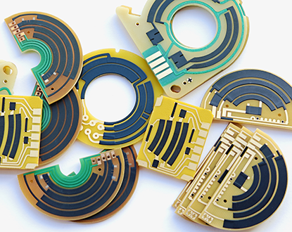
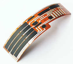
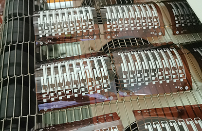
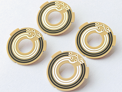
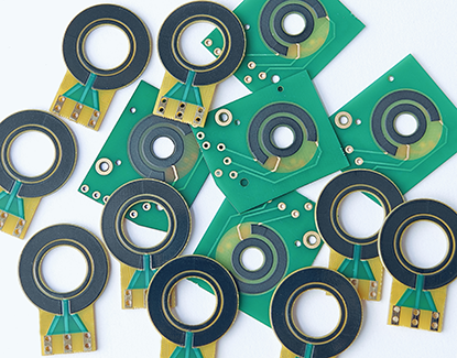
Thick Film Potentiometer PCB
Thick Film Potentiometer PCBs are specialized electronic components that integrate variable resistors into printed circuit boards, using thick film technology where conductive, resistive, and insulating materials are sequentially applied to PI, FR4, or ceramic PCBs, followed by high-temperature sintering and laser trimming to create precise, reliable potentiometers for efficient and customizable solutions in various electronic systems. Thick Film Potentiometer PCBs can achieve all the functions of linear potentiometer, rotary potentiometer and logarithmic taper potentiometer, which is equivalent to transplanting or integrating the potentiometer module directly onto the PCB surface. It can not only effectively save the assembly space of the products, but also provide a variety of options for product developers, The most important thing is to reduce the manufacturing cost effectively. Thick Film Potentiometer PCBs offer several advantages, including high precision, flexibility, stability, and the ability to integrate multiple resistors on a single substrate. This makes thick film potentiometer PCBs suitable for a wide range of applications, including in electronic sensors, industrial controls, automotive systems, and more. Features of Thick Film Potentiometer PCB : |
 |
|
 |
1, Adjustable Resistance: Thick film potentiometer PCB allowed to adjust the resistance value by applying a sliding contact or wiper along the resistive element. This allows for precise control over the resistance in the circuit. 2, Resistive Element: Thick film potentiometer PCB consists of a resistive element printed on the surface of the PCB using a thick film printing process. This resistive element acts as the variable resistance. 3, Temperature Stability: Thick film potentiometer PCBs exhibit good temperature stability, ensuring that the resistance remains consistent even with variations in temperature. 4, High Power Handling Capability: Thick film potentiometer PCBs can handle high power levels, making them suitable for applications of high-power dissipation. |
|
5, Linear and Logarithmic Taper: Thick film potentiometer PCBs are available in both linear and logarithmic taper options. Linear taper provides a constant rate of resistance change, while logarithmic taper provides a logarithmic response, commonly used in audio applications to control volume. 6, Compact Size: Thick Film Potentiometric Sensors are designed to be compact and fit easily on a circuit board. They have a small footprint, making them suitable for space-constrained applications. 7, Longevity: Thick film potentiometer PCBs have a long operational life due to the durable nature of the thick film resistive material used. This ensures reliable performance and longevity in various applications. 8, Wide Range of Resistance Values: Thick film potentiometer PCBs are available in a wide range of resistance values, from a few ohms to several megaohms. This allows for versatile usage in different circuit designs. 9, Cost-Effective: Thick film potentiometer PCBs are cost-effective compared to other types of potentiometers, making them a preferred choice for various consumer electronics and industrial applications. 10, Easy Integration: Thick film potentiometer PCBs can be easily integrated into electronic circuits during the PCB assembly process, simplifying the manufacturing. Please refer to Thick Film Resistor PCB for more informations. |
||
Typical Applications of Thick Film Potentiometer PCB : |
1, Automotive Electronics: Thick film potentiometer PCBs are used in automotive applications for functions like controlling the audio system, adjusting HVAC settings, throttle position sensor, and operating dashboard controls. 2, Aerospace and Defense: Thick film potentiometric sensors are used in aerospace and defense applications, including flight control systems, radar systems, and military communication equipment. They ensure precise control and reliable operation in demanding environments. |
|
 |
3, Consumer Electronics: Thick film potentiometer PCBs are utilized in a wide range of consumer electronics, including televisions, radios, home theater systems, and portable audio players. They enable adjustment of settings like brightness, contrast, and tone. 4, Instrumentation: Thick film potentiometer PCBs are used in instrumentation devices where precise control of electrical parameters is required. They can be found in devices such as oscilloscopes, signal generators, and data acquisition systems. 5, Industrial Controls: Thick film potentiometer PCBs are employed in various industrial control systems that require precise adjustment and monitoring of parameters. These include motor speed controllers, robotic systems, and automation equipment. 6, Communication Systems: Thick film potentiometer PCBs are employed in communication systems such as modems, routers, and telecommunication devices. They facilitate adjustment of signal strength, frequency, and other communication parameters. |
7, Energy Systems: Thick film potentiometer PCBs play a role in energy systems, including solar power inverters, battery management systems, and power distribution equipment. They enable adjustment and monitoring of electrical parameters. 8, Audio Equipment: Thick film potentiometer PCBs are commonly used in audio equipment such as amplifiers, mixers, and preamps. They can control volume levels and provide precise audio adjustments. 9, Medical Devices: Thick film potentiometer PCBs use in medical devices such as diagnostic equipment, patient monitoring systems, and surgical instruments. They enable fine adjustment of settings and parameters. |
|
Applications in Automotive of Thick Film Potentiometer PCB : |
Thick Film Potentiometer PCBs find various applications in automotive electronics, including throttle position sensors, steering angle sensors, HVAC control, headlight leveling systems, and power seat adjustment systems. These applications contribute to improved performance, safety, and comfort in vehicles. 1, HVAC Control: Another application of thick film potentiometer PCBs in automotive electronics is HVAC (Heating, Ventilation, and Air Conditioning) control systems. These systems regulate the temperature and airflow inside the vehicle cabin. The potentiometer on the PCB can be used to adjust the fan speed and temperature settings based on user input. By accurately sensing the position of the control knobs or buttons, the potentiometer helps to maintain the desired comfort level inside the vehicle. |
|
 |
2, Throttle Position Sensor: Thick film potentiometer PCBs can be used in throttle position sensors in automotive electronics. Throttle position sensors detect the position of the throttle valve in the engine. The potentiometer on the PCB measures the resistance change as the throttle valve is moved, providing accurate feedback to the engine control unit (ECU) about the throttle position. This information is crucial for controlling the fuel injection and ignition timing of the engine, ensuring optimal performance and fuel efficiency. 3, Steering Angle Sensor: Thick film potentiometer PCBs can also be employed in steering angle sensors in automobiles. These sensors detect the angle at which the steering wheel is turned by measuring the resistance change in the potentiometer as the steering wheel rotates. This data is utilized by the vehicle's stability control system to determine the intended direction of the vehicle and apply appropriate corrective measures if necessary. Accurate steering angle measurement is critical for enhancing vehicle safety and stability. |
4, Headlight Leveling System: Thick film potentiometer PCBs are also utilized in headlight leveling systems. These systems automatically adjust the height of the headlights based on the vehicle's pitch and roll angles. The potentiometer on the PCB measures the inclination of the vehicle and provides feedback to the headlight control unit. This enables the headlights to be positioned correctly, ensuring optimal visibility without dazzling oncoming drivers. 5, Power Seat Adjustment: Thick film potentiometer PCBs can be integrated into power seat adjustment systems in automobiles. These systems allow the driver and passengers to adjust the position and angle of their seats for optimal comfort. The potentiometer on the PCB measures the seat position and provides feedback to the seat control unit. This enables precise seat adjustments based on user preferences. These applications demonstrate the versatility and importance of thick film potentiometer PCBs in various automotive electronic systems. |
|
Manufacturing Challenges of Thick Film Potentiometer PCB : |
Manufacturing a Thick Film Potentiometer PCB presents certain challenges due to the specific nature of their construction and materials. These challenges include: 1, Process Complexity: The manufacturing process for thick film potentiometer PCBs involves multiple intricate steps, including screen printing, firing, and trimming. Each step requires precise control and coordination to ensure accurate resistance values and optimal performance. |
|
 |
2, Material Selection: The selection of suitable materials for the thick film resistive layer is crucial to achieve desired electrical characteristics and long-term stability. Finding materials that exhibit low temperature coefficient of resistance (TCR) and high reliability can be challenging. 3, Uniformity and Consistency: Achieving uniformity and consistency in the resistive layer thickness and composition across the entire PCB is critical. Any variations in these parameters can lead to inaccuracies in resistance values and affect the overall performance of the potentiometer. 4, Firing and Laser Trimming: The firing process, which involves heating the PCB to a specific temperature, requires careful control to ensure proper adhesion of the resistive layer to the substrate. The trimming process, where excess resistive material is removed to achieve the desired resistance value, demands precision. 5, Reliability Testing: Thick film potentiometer PCBs must undergo rigorous reliability testing to verify their performance under different operating conditions, such as temperature variations, humidity, and mechanical stress. This testing ensures that the potentiometers meet the required standards for durability and long-term functionality. |
6, Quality Assurance: Implementing robust quality control measures throughout the manufacturing process is essential to identify and rectify any defects or inconsistencies. This includes extensive testing and inspection of the resistive layer, substrate, and overall PCB assembly. |
|
Main Types of Thick Film Potentiometer PCB : |
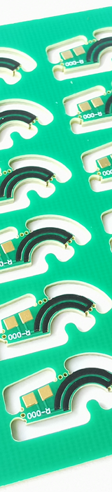
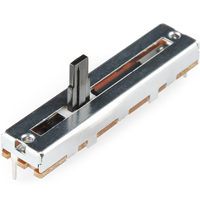
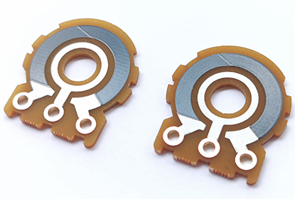
1, Linear Potentiometer PCB : Combine the conductive carbon element onto the PCB, consist of a linear slider that controls the position of the wiper, Sliding along the thick film carbon resistor printed on the PCB. |
Types of Linear Potentiometer PCB : |
 |
Linear Potentiometer PCB also called slider or fader potentiometers, consist of an adjustable multi-wire wiper that moves in a linear motion. Linear potentiometers PCB are commonly used to measure the resistance of voltage. The thick film resistive material is printed to a track alongside which the multi-wire wiper moves. Linear potentiometers PCB are further divided into four types: |
Types |
Description |
Applications |
Slide pot |
Single linear slider potentiometer, for audio applications also known as a fader. High quality faders are often constructed from conductive plastic. |
For single channel control or measurement of distance. |
Dual-slide pot |
Dual slide potentiometer, single slider controlling two potentiometers in parallel. |
Often used for stereo control in professional audio or other applications where dual parallel channels are controlled. |
Multi-turn slide |
Constructed from a spindle which actuates a linear potentiometer wiper. Multiple rotations (mostly 5, 10 or 20), for increased precision. |
Used where high precision and resolution is required. The multi turn linear pots are used as trimpots on PCB, but not as common as the worm-gear trimmer potentiometer. |
Motorized fader |
Fader which can be automatically adjusted by a servo motor. |
Used where manual and automatic adjustment is required. Common in studio audio mixers, where the servo faders can be automatically moved to a saved configuration. |
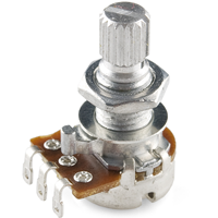
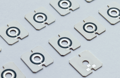
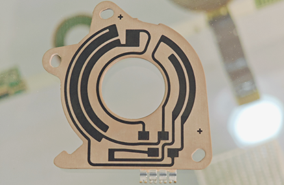
Types of Rotary Potentiometer PCB : |
 |
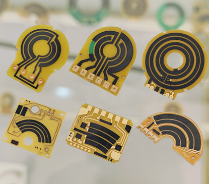
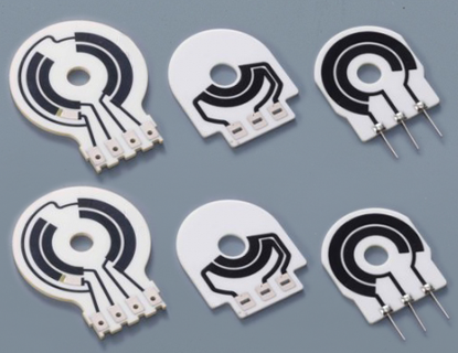
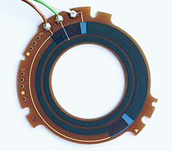
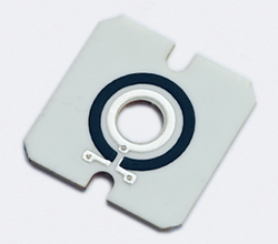
Rotary Potentiometer PCBs are the most common types of potentiometers used. They consist of an adjustable wiper that moves in a circular motion when turning the knob, The thick film resistive material is printed in a semi-circular pattern between the two terminals, They are primarily used to obtain an adjustable supply of voltage,The rotary potentiometers PCB are divided into five types: |
Types |
Description |
Applications |
Single-turn pot |
Single rotation of approximately 270 degrees or 3/4 of a full turn |
Most common pot, used in applications where a single turn provides enough control resolution. |
Multi-turn pot |
Multiple rotations (mostly 5, 10 or 20), for increased precision. They are constructed either with a wiper that follows a spiral or helix form, or by using a worm-gear. |
Used where high precision and resolution is required. The worm-gear multi turn pots are often used as trimpots on PCB. |
Dual-gang pot |
Two potentiometer combined on the same shaft, enabling the parallel setting of two channels. Most common are single turn potentiometers with equal resistance and taper. More than two gangs are possible but not very common. |
Used in for example stereo audio volume control or other applications where 2 channels have to be adjusted in parallel. |
Concentric pot |
Dual potmeter, where the two potentiometers are individually adjusted by means of concentric shafts. Enables the use of two controls on one unit. |
Often encountered in (older) car radios, where the volume and tone controls are combined. |
Servo pot |
A motorized potmeter which can also be automatically adjusted by a servo motor. |
Used where manual and automatic adjustment is required. Often seen in audio equipment, where the remote-control can turn the volume control knob. |
How Does Thick Film Potentiometer PCB Work ? |
● Linear Potentiometer PCB works by having a resistive element on the PCB. Both end terminals are attached to thick film resistor, The wiper travels along the resistor strip when the knob is moved. The closer the multi-wire wiper is to the end terminal it is wired in conjunction with, the less the resistance, because the path of the current will be shorter. The further away it moves from the terminal, the greater the resistance will be. For example, when the sliding contact is at the middle position, the variable resistance value is half of the full-scale resistance of the potentiometer. In these types of potentiometers, the multi-wire wiper moves along a linear path. Also known as slide pot, slider, or fader. This potentiometer is similar to the rotary-type but in this potentiometer, the sliding wiper simply rotated on the resistor linearly. The connection of the resistor’s two terminals is connected across the voltage source. A sliding wiper on the resistor can be moved using a path that is connected through the resistor. |
|
● Rotary Potentiometer PCB uses a strip of carbon resistive material with constant density all the way around. The resistance between the center terminal and either end terminal changes at a steady rate as the control shaft rotates, The resistance between the middle terminal and-either end terminal constitutes a linear finction of the angular shaft position. In the majority of variable resistors available this is a linear relationship, meaning that the relative position is equal to the resistance ratio. This kind of potentiometer includes two terminal contacts where a consistent resistance can be located in a semi-circular model. And also it includes a terminal in the middle that is allied to the resistance using a sliding wiper that is connected through a rotating knob. The sliding wiper can be turned by turning the knob over the half-circular resistance. The voltage of this can be obtained among the two contacts of resistance & the sliding. These rotary potentiometer PCBs are used wherever level voltage control is necessary. |
|
Materials Selection of Thick Film Potentiometer PCB : |
Substrates |
Advantages |
Disadvantages |
|
FR4 |
|
● Cost-Effectiveness: FR4 is the most common PCB substrate material, and due to its widespread use, it is relatively low in cost. ● Good Electrical Properties: FR4 has good insulation and mechanical strength, making it suitable for most electronic applications. ● Easy to Process: FR4 is easy to manufacture and fabricate, compatible with various PCB production techniques. |
● Limited Heat Resistance: Although FR4 can operate at higher temperatures, it has lower heat resistance compared to ceramic substrates. ● Relatively High CTE: This can affect the stability of the circuit under temperature changes. |
Ceramic |
|
● High Thermal Conductivity: Ceramic substrates have excellent thermal conductivity, which is helpful for heat dissipation and suitable for high-power applications. ● Good Electrical Insulation: Ceramic materials have high electrical insulation properties, making them ideal for high-frequency circuits. ● Thermal Stability: Ceramics have a low coefficient of thermal expansion, making them suitable for operation under extreme temperatures. |
● Higher Cost: Compared to FR4, ceramic substrates are more expensive. ● Processing Difficulty: Due to the high hardness of ceramic materials, they are more difficult and costly to process. |
Flex PI |
|
● Flexibility: PI substrates have good flexibility, making them suitable for applications that require bending or curling. ● High-Temperature Resistance: PI substrates can operate stably in high-temperature environments. ● Chemical Resistance: PI substrates have good resistance to a variety of chemicals. |
● Higher Cost: The cost of PI substrates is usually higher than that of FR4. ● Electrical Properties: Although PI substrates have excellent mechanical properties, their electrical properties may not be as good as those of ceramic substrates. |
When selecting a substrate material for Thick Film Potentiometer PCBs, it is necessary to balance the specific requirements of the application and the budget. For instance, if the application requires high power handling and excellent heat dissipation, ceramic might be a better choice. If considering a balance between cost and electrical performance, FR4 might be a more suitable choice. For applications requiring flexibility, PI substrates are the ideal choice. |
|||
Conductive Paste of Thick Film Potentiometer PCB : |
1, High Conductivity: The conductive paste exhibits high electrical conductivity due to the presence of metal powders, such as ruthenium, palladium, silver, or a combination thereof. This high conductivity allows for accurate measurement and control of electrical signals in the potentiometer. 2, Uniform Particle Size Distribution: The conductive paste possesses a uniform particle size distribution of the metal powders. This ensures consistent conductivity and resistance values across the resistive layer, enabling precise control and accurate measurement in the potentiometer. |
|
 |
3, Excellent Adhesion: The conductive paste demonstrates excellent adhesion to the substrate material, ensuring a strong bond between the resistive layer and the PCB. This reliable adhesion prevents delamination and ensures long-term stability and durability of the potentiometer. 4, Thermal Stability: The conductive paste exhibits excellent thermal stability to withstand the high temperatures encountered during the firing process. It maintains its structural integrity and conductivity even under prolonged exposure to elevated temperatures, ensuring reliable performance in demanding operating conditions. 5, Chemical Compatibility: The conductive paste is chemically compatible with the substrate material, preventing any adverse reactions or degradation over time. This compatibility ensures the long-term reliability and functionality. |
6, Adjustable Rheological Properties: The conductive paste can be formulated with adjustable rheological properties to facilitate its application through screen printing. It possesses the ideal viscosity and flow characteristics to ensure smooth and uniform printing onto the substrate, enabling consistent resistive layer formation. 7, Optimized Drying Behavior: The conductive paste exhibits optimized drying behavior, allowing it to dry evenly and efficiently during the manufacturing process. This ensures consistent quality and minimizes defects or variations in the resistive layer. |
|
Resistive Paste of Thick Film Potentiometer PCB : |
1, Low Voltage Coefficient of Resistance (VCR): This paste exhibits a low voltage coefficient of resistance (VCR) and minimal noise, making it particularly suitable for printed carbon potentiometers. It ensures stable and accurate voltage division, key for potentiometer functionality. |
|
 |
2, Stability of Resistance Values, Especially at High Temperatures: These pastes offer exceptional stability of resistance values, even at elevated temperatures, making them ideal for applications requiring consistent linearity, such as linear position sensors. 3, Low Temperature Coefficient of Resistance (TCR) and Good Reproducibility: The paste demonstrates a low temperature coefficient of resistance (TCR) and excellent reproducibility of TCR, ensuring precise tracking of resistance values among resistors on the same substrate. 4, Wide Range of Sheet Resistivity: The paste provides a broad range of sheet resistivity, enabling its use in thick film resistor PCBs, thick film heaters, and thick film potentiometer PCBs, catering to diverse electrical requirements. |
5, Compatibility with Conductor Paste Systems: It is compatible with conductor paste systems, particularly suitable for thick film ceramic PCBs like APM PCB, ensuring seamless integration into complex circuit designs. 6, Less Sensitive to Firing Profile Variations: These modern pastes are less sensitive to variations in the firing profile compared to earlier formulations, delivering improved TCR and stability performance. They are primarily based on oxides of ruthenium, iridium, and rhenium, with TCR performance linked to sheet resistivity, achieving optimal results within the 1kΩ/sq. to 10kΩ/sq. and 10MΩ/sq. range. |
|
Dielectric Paste of Thick Film Potentiometer PCB : |
1, High Dielectric Strength: This dielectric paste exhibits high dielectric strength, enabling its application between two conductor layers as an insulating layer in multilayer hybrid circuits. It ensures reliable isolation and electrical integrity within complex circuit designs. 2, Good Insulation Resistance: The paste offers good insulation resistance, allowing it to be printed and overlaid on conductor layers as a protective barrier. This feature enhances the durability and longevity of the PCB by safeguarding against external factors. |
|
 |
3, Low Power Factor: With a low power factor, this paste can be applied on a metal core (such as stainless steel) as an insulating layer for thick film heating elements. This property is essential for maintaining efficient and stable performance in heating applications. 4, High Dielectric Constant: In the fabrication of thick film resistor elements, a high dielectric constant is beneficial for achieving stability. A dielectric constant of around 10 is typically considered optimal to avoid thermal coefficient issues, as materials with higher dielectric constants may introduce undesirable thermal effects. 5, Thermal Stability: The dielectric paste should possess excellent thermal stability to withstand varying temperatures during operation without compromising its insulating properties. This ensures consistent performance in different thermal environments. |
6, Adhesion Strength: A crucial characteristic is the adhesion strength of the dielectric paste to the substrate and other layers within the PCB. Strong adhesion prevents delamination and ensures the integrity of the entire circuit structure. 7, Chemical Resistance: It is essential for the dielectric paste to exhibit high chemical resistance to withstand exposure to potentially corrosive substances or environments. This property prolongs the lifespan of the PCB and maintains its functionality over time. |
|
Linearity Definition of Thick Film Potentiometer PCB : |
 |
1, The linearity of potentiometer sensor is the deviation of the output characteristic curve as compared to an ideal straiaht line, It is measured by the greatest deviation from the ideal straight line with respect to the applied voltage, High precision linearity is a key factor to ensure a stable voltage output of potentiometer. 2, The deviation is given in %, For example, to be 1.0%, or 0.5%, Essentially three types ofnonlinearities can be provided for potentiometer sensor specifications. The required type of linearity and linearity deviation should always be customized for the each specific application. |
3, The linearity of thick film potentiometer PCB refers to the degree to which the relationship between the resistance value and the position of the wiper element is linear. In other words, it measures how closely the output voltage or resistance changes in proportion to the physical displacement of the wiper along the potentiometer track. 4, A perfectly linear potentiometer sensor would exhibit a consistent and predictable change in resistance or voltage as the wiper is moved across the entire range. However, in reality, there may be some deviations from linearity due to various factors such as manufacturing tolerances, materials used, or mechanical limitations. |
|
Why Linearity Important for Thick Film Potentiometer PCB ? |
● The Linearity of a linear, rotary potentiometric sensors or position sensors refer to how closely the resistance changes in relation to the movement of the wiper or slider along the resistor's surface, It measures the degree to which the resistance follows a linear relationship with the position of the wiper. A resistor with high linearity will exhibit a consistent and predictable change in resistance as the wiper moves, adhering closely to a linear relationship. Conversely, a resistor with poor linearity may deviate from this linear relationship, resulting in non-linear changes in resistance across its range. ● A smaller linearity value indicates that the change in resistance across the Potentiometric Sensor's entire range is more consistent, adhering closely to a linear relationship. This consistency results in a more precise and stable voltage (or signal) output. In simpler terms, a lower linearity value means that minor positional adjustments of the wiper lead to proportional and predictable changes in output voltage. |
|
 |
● Conversely, a larger linearity value suggests potential deviations from a linear resistance change as the wiper moves, introducing non-linearities and inconsistencies in the voltage output, which diminish precision and stability. ● Therefore, achieving a lower linearity value in a linear potentiometers PCB or rotary potentiometer PCB is crucial for ensuring accurate and stable voltage outputs, thus guaranteeing reliable performance across various applications. ● During our production of potentiometer PCB or position sensor PCB, a one-time carbon printing process can achieve a standard resistance tolerance of ±10% with a linearity of ±1.0% without laser trimming. If customers require linearity of < 1.0% (e.g., 0.5% or 0.25%), then laser trimming becomes necessary for adjusting linearity. For example, under our normal processes, a one-time carbon printing process can achieve a standard resistance tolerance of : |
If the customer requires a linearity of <1.0%, then the resistance tolerance must be adjusted from ±10% to ±15% or +/-20%, Then it is to be : ● When using laser trimming to achieve lower linearity, the resistance value continuously fluctuate along with the entire process of laser trimming (the resistance increases over time). Therefore, in such conditions, it becomes unreasonable to demand a high precision (tolerance) controlling of the resistance value , as it hinders the attainment of better linearity. On the contrary, as the consistency of linearity improves, it is generally preferred to relax the resistance tolerance range and ensuring the manufacturability of laser trimming. Ensuring good linearity takes precedence over precise control of the resistance value in the production of potentiometers. ● It's important to note that while resistance tolerance is a factor in determining a resistor's overall precision, But it is not the primary determinant of voltage output stability. In essence, if the resistor design incorporates linear functionality, controlling a lower linearity tolerance becomes more critical than managing resistance tolerance. |
|
Why Deed to Customize Thick Film Potentiometer PCB ? |
● Specific Requirements: Different applications have unique requirements for resistance, tolerance, temperature range, and environmental conditions. Customizing Thick Film Potentiometer PCB allows for the creation of potentiometers that meet these specific needs. ● Optimized Performance: A customized Thick Film Potentiometer PCB can be designed to optimize the performance of the potentiometer, ensuring it operates efficiently within the desired parameters. ● Space Constraints: In many electronic devices, space is at a premium. Customizing the Thick Film Potentiometer PCB allows for the creation of potentiometers that fit precisely into the available space without compromising functionality. |
|
 |
● Integration: Potentiometer PCB can be designed to integrate seamlessly with other components on the board, reducing the need for additional wiring or connectors. ● Cost Efficiency: While there may be an initial cost associated with customizing a PCB, it can lead to cost savings in the long run by reducing the need for multiple components or by improving the efficiency of the overall system. ● Quality Control: Customizing a Thick Film Potentiometer PCB allows for better quality control, as the manufacturer can ensure that the potentiometer meets all the necessary standards and specifications. ● Reliability: A customized potentiometer can be designed to be more reliable and durable, withstanding the rigors of the application it is designed for. ● Custom Features: Custom Thick Film Potentiometer PCBs can include features such as specific mounting options, unique form factors, or additional electronic components that are not available in standard products. |
● Rapid Prototyping: For new product development, custom potentiometer PCBs can be rapidly prototyped and tested, speeding up the development process. ● Competitive Advantage: Offering custom potentiometers can give a company a competitive edge by providing products that are tailored to the customer's exact needs. Customizing a Thick Film Potentiometer PCB is about ensuring that the potentiometer is fit for purpose, optimized for performance, and integrated efficiently into the end product. |
|
Logarithmic Taper Potentiometer PCB : |
Logarithmic Taper Potentiometers PCB, or called Non-Linear Potentiometer PCB is particularly well-suited for applications in audio equipment, such as volume controls and audio signal fade-in/fade-out or balance adjustments. This suitability arises from the logarithmic nature of human auditory perception, where changes in sound intensity are perceived logarithmically rather than linearly. As a result, logarithmic taper potentiometers provide a more natural and smooth volume adjustment experience, making them ideal for various audio applications. Furthermore, Logarithmic Taper Potentiometers PCB is commonly used in other applications that require the simulation of human hearing characteristics, such as specific industrial control systems that necessitate precise auditory control. |
|
 |
Logarithmic Taper Potentiometers PCB, or Audio Taper Potentiometer PCB is a type of printed circuit board that employs thick film resistor technology, featuring resistance values that change according to a logarithmic scale. In the manufacturing process, resistor paste is printed onto a FR4 or ceramic substrate using screen printing techniques, followed by high-temperature sintering to form the resistor layer. This is further refined through laser trimming to ensure precise resistance values, guaranteeing accuracy in electronic applications. Logarithmic Potentiometers PCB serve as the support for electronic components and the medium for their electrical connections. Logarithmic Taper Potentiometers PCB design and manufacturing must consider factors such as circuit functionality, component layout, wiring rationality, and electromagnetic compatibility to ensure the stability and reliability of the circuit. Some features of Logarithmic Potentiometers PCB as followings: |
● Logarithmic Potentiometer Installation: The PCB is equipped with logarithmic taper potentiometers, which have resistance values that change according to a logarithmic scale. This feature makes them particularly suitable for applications such as volume control, where human auditory perception is logarithmic. ● Circuit Design: The circuit design on logarithmic taper potentiometer PCBs takes into account the unique characteristics of these potentiometers, such as resolution, end-to-end resistance, and compatibility with other electronic components. This ensures optimal performance and functionality. ● Digital Interfaces: Some logarithmic taper potentiometer PCBs may incorporate digital interfaces, such as SPI (Serial Peripheral Interface) or I2C (Inter-Integrated Circuit), enabling precise control and easier integration with microcontrollers and digital systems. ● Multiple Packaging Options: These Logarithmic Taper Potentiometers PCBs often provide various packaging options to accommodate different applications and space requirements, offering flexibility in design and implementation. ● Low Power Design: Many logarithmic taper potentiometer PCBs are designed with low power consumption in mind, reducing energy usage and extending the lifespan of the device. ● High Reliability: The design of logarithmic taper potentiometer PCBs emphasizes high reliability, including durability and data retention time, to ensure consistent operation over time. ● Wide Applications: Logarithmic taper potentiometer PCBs find extensive use in fields such as audio equipment, medical devices, and industrial control systems, particularly in applications requiring logarithmic response characteristics. |
|
Multi-Wire Wipers Used For Thick Film Potentiometer PCB : |
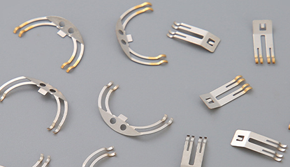 |
Multi-Wire Wipers are crucial components designed to transmit voltage and signals. They perform linear or rotational sliding over the surfaces of resistive materials (thick film resistors) to adjust resistance values and act as contact elements in voltage dividers. Wiper design is extremely critical for the efficiency and life of the sensor assembly, When designing the wiper, it is very important to consider contact resistance, working-hight (load), repeatability, hysteresis, the resistive material used, and in particular, the wiper material itself, its shape and the wiper pressure. We also provided custom Multi-Wire Wipers (Contact) for customer if needs, we can manufacture the wipers according to customer's design requirements or specification, For more information about wipers, Please refer to Multi-Contact Wipers. |
Engineering Specification of Thick Film Potentiometer PCB : |
Items : |
Typical Values |
Advanced Capabilities |
1, Substrates : |
FR4, Ceramic ( AI203, ALN, BeO, ZrO2), Polyimide (Flexible PI), Stainless Steel (SUS304), Mica |
FR4, Ceramic ( AI203, ALN, BeO, ZrO2), Polyimide (Flexible PI), Stainless Steel (SUS304), Mica |
2, Conductor (Paste) Materials : |
Copper, Silver , Gold , Silver-Palladium, Palladium-Gold, Platinum-Silver, Platinum-Gold |
Copper, Silver , Gold , Silver-Palladium, Palladium-Gold, Platinum-Silver, Platinum-Gold |
3, Thick Film Carbon Thickness (Height) : |
15um +/-5 um |
30um +/-5 um |
4, Conductor Thickness (Height) : |
12um+/-5um |
20um+/-5um |
5, Min Width of Thick Film Line : |
0.30 mm +/-0.05 mm |
0.20 mm +/-0.05 mm |
6, Min Space of Thick Film Line : |
0.30 mm +/-0.05 mm |
0.20 mm +/-0.05 mm |
7, Min Overlap (Carbon to Conductor) : |
No less than 0.25mm |
0.20mm (Minimum) |
8, Sheet Resistivity (ohms/square): |
Printed resistors in milli ohm to mega ohm range (Customizable) with tolerances of 1-10% are fabricated and protected with overglaze materials. |
Printed resistors in milli ohm to mega ohm range (Customizable) with tolerances of 0.5-10% are fabricated and protected with overglaze materials. |
9, Resistor Value Tolerance (ohms) : |
+/-10.0% (Standard) (Customizable) |
+/-0.5% (Laser trimming) |
10, Linearity : |
+/-1.0% (Standard) (Customizable) |
+/-0.2 ~ +/-0.5% (Laser trimming) |
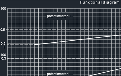
11, Synchronism of Double Channels : |
+/-2.0% (Standard) (Customizable) (Potentiometers) |
+/-1.0% (Laser trimming) (Potentiometers) |
12, Durability of Carbon Ink (Life time) : |
0.5 Million (Min), 2.0 Million (Standard) |
5.0-10.0 Million (Max) with Surface Polishing |
13, Working Temperature : |
- 40ºC /+150ºC |
- 40ºC /+180ºC |