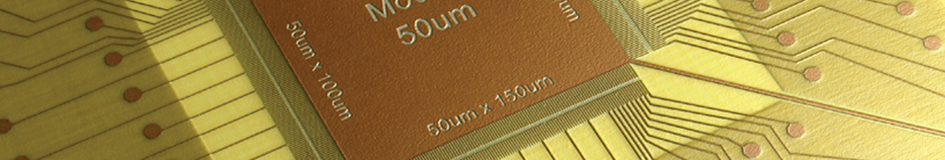
Embedded Resistor PCB
Embedded Resistor PCBs are advanced electronic circuits that use thin film technology to embed resistors inside the PCB, with the manufacturing process involving bonding a thin film of resistive material (such as nichrome alloy or tantalum nitride) to the PCB's inner core through a vacuum hot-press process, followed by pattern transfer and etching to precisely create the required resistor elements, after which additional layers are added to form a tightly integrated circuit system that embeds the resistors, eliminating the need for discrete resistive components in traditional methods and enhancing resistance control precision. Embedded Resistor PCBs are characterized by the direct integration of resistive elements into the PCB substrate, eliminating the need for external resistive components. This design not only saves space but also reduces the number of components, thus simplifying the circuit and lowering assembly costs. Additionally, Embedded Resistor PCBs provide superior electrical performance, as thin-film technology enables precise resistance value control, ensuring circuit reliability and stability. The close integration of resistive elements with other circuit components also improves signal transmission and heat management. Embedded Resistor PCBs are widely used in high-density electronic devices, especially in applications where space is limited and high performance is required. They are commonly found in consumer electronics, communication equipment, automotive electronics, and medical instruments. In these applications, Embedded Resistor PCBs offer smaller and more efficient circuit designs, meeting the demands for miniaturization, integration, and high reliability in modern electronic products. Furthermore, they are often used in high-frequency circuits and precision instruments that require accurate resistance values, such as RF circuits, sensor modules. Main Features of Embedded Resistor PCB : |
 |
|
 |
1, Integration for High-Speed, High-Density Devices: 2, Enhanced Bonding Properties with Thin Film Resistor Foil: |
|
3, Technology Options of Embedded Resistor PCB: Thin Film vs. Thick Film: 4, Factors Impacting Resistance Value in Thin Film Resistors: |
||
How to Calculate Resistor Value of Embedded Resistor PCB : |
Calculating the resistor value for an embedded resistor in a Printed Circuit Board (PCB) involves understanding the specific requirements of your circuit, including the desired resistance value, the tolerance levels acceptable for your application, and the physical constraints of your PCB design. Embedded resistors in PCBs are part of the board material itself and are designed to save space and improve performance by integrating passive components directly into the PCB. Here’s a step-by-step guide to help you calculate the resistor value for an embedded resistor PCB: 1. Determine the Required Resistance Value: |
|
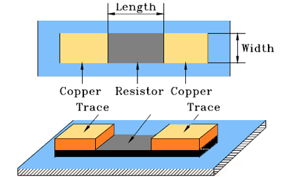 |
2. Understand the Material Properties: |
To be simple, All resistor materials are provided with resistance values expressed in ohms per square as : R = pL/A, R is resistance in ohms, p is the resistivity of the material, L is the length and A is the cross sectional area (i.e., thickness times width). When thickness is held constant then R is the same for any square area, hence the expression ohms/square. Resistance then can be varied by varying the aspect ratio of the area (L/W). 3. Adjust for Manufacturing Tolerances: 4. Calculate the Desired Geometry: 5. Verify and Test: |
|
What is the Resistive Foil Material in Embedded Resistor PCB ? |
1, Composition and Characteristics: |
|
 |
2, Selection Criteria for Resistive Material: 3, Manufacturing Process: |
4, Application and Etching: 5, Material Options for Embedded Resistor PCBs: |
|
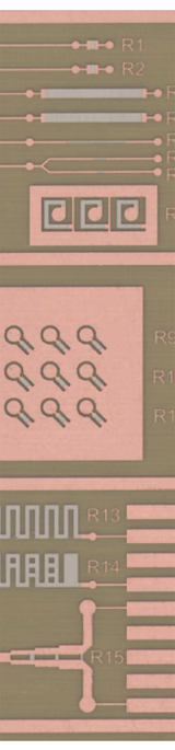
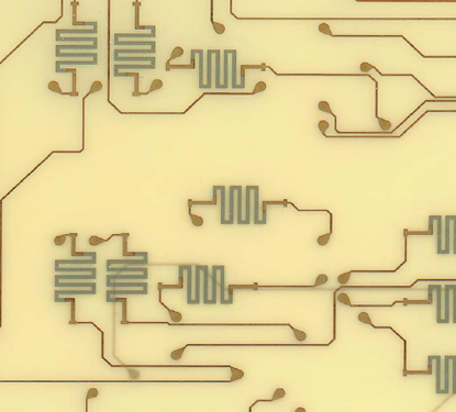
Advantages of Embedded Resistor PCB : |
Embedded resistor technology in Printed Circuit Boards (PCB) integrates resistors directly into the PCB structure, offering several advantages over traditional surface-mounted or through-hole resistors. This integration can lead to improvements in performance, reliability, and design flexibility, among other benefits. Here are some of the key advantages: 1. Space Saving: One of the most significant advantages of embedded resistor PCBs is the conservation of board space. By integrating resistors within the PCB layers, the need for surface-mounted or through-hole components is reduced, freeing up space for other components or enabling the design of smaller, more compact PCBs. This is particularly beneficial in applications where space is at a premium, such as in mobile devices or wearable technology. 2. Improved Electrical Performance: Embedded resistors can enhance the electrical performance of a circuit. They reduce the parasitic inductance and capacitance associated with discrete components, leading to better signal integrity and faster signal propagation. This is crucial for high-speed or high-frequency applications where maintaining signal integrity is essential. |
|
 |
3. Enhanced Reliability: Integrating resistors into the PCB can improve the overall reliability of the electronic device. Embedded resistors are less susceptible to mechanical stress and thermal cycling, which can affect surface-mounted components. This integration reduces the risk of component failure due to physical stress or solder joint issues, leading to longer-lasting and more reliable products. 4. Reduced Assembly Time and Cost: By reducing the number of discrete components that need to be placed and soldered onto the PCB, embedded resistor technology can streamline the assembly process. This not only speeds up production but can also lower assembly costs. Fewer components mean fewer opportunities for assembly errors, contributing to higher yield rates and reduced rework costs. 5. Improved Thermal Management: Embedded resistors can contribute to better thermal management within a PCB. Since they are part of the PCB structure, they can dissipate heat more effectively than surface-mounted resistors, which often require additional thermal management solutions. Effective heat dissipation is critical for maintaining the performance and longevity of electronic devices. |
6. Design Flexibility: The use of embedded resistors offers greater design flexibility. Designers can place resistors exactly where needed without being constrained by the layout limitations of surface-mounted or through-hole components. This flexibility can lead to more efficient use of space and optimized circuit performance. 7. Reduced Signal Paths: Incorporating resistors directly into the PCB substrate can shorten signal paths, reducing signal degradation and improving the overall performance of the electronic device. Shorter signal paths are particularly beneficial in high-speed applications where every fraction of a nanosecond counts. Embedded resistor technology in PCBs provides significant advantages in terms of space utilization, electrical performance, reliability, production efficiency, thermal management, design flexibility, and signal integrity. These benefits make it an attractive option for a wide range of applications, particularly where performance and miniaturization are critical. |
|
Applications of Embedded Resistor PCB : |
Embedded resistor PCBs have found applications across a wide range of industries, leveraging their advantages to enhance performance, reliability, and compactness in electronic devices. Here are some of the key applications: 1. Consumer Electronics 2. Aerospace and Defense 3. Automotive Electronics |
|
 |
4. Medical Devices 5. High-Frequency Applications 6. Industrial Automation and Control Systems |
7. Computing and Networking 8. Wearable Technology 9. Power Electronics The applications of embedded resistor PCBs span various sectors, offering significant benefits in terms of reliability, performance, and compactness. Their use is particularly advantageous in applications where space constraints, environmental conditions, and high-performance requirements challenge traditional PCB designs. |
|
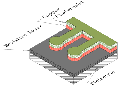
Etching Sequence Schematic of Embedded Resistor PCB : |
The etching sequence for creating an embedded resistor in a PCB involves several critical steps, designed to integrate the resistor directly into the PCB structure. This process requires precise control over materials and etching parameters to achieve the desired resistor values and ensure the integrity of the final product. Below is a simplified schematic of the etching sequence for an embedded resistor PCB: 1. Preparation of Copper Foil 2. Deposition of Resistive Material |
|
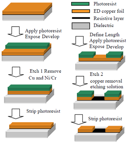 |
3. Application of Photoresist 4. Etching of Resistive Layer 5. Stripping and Final Etching |
6. Passivation and Finishing |
|
Multiple Sheet Resistivities of Embedded Resistor PCB : |
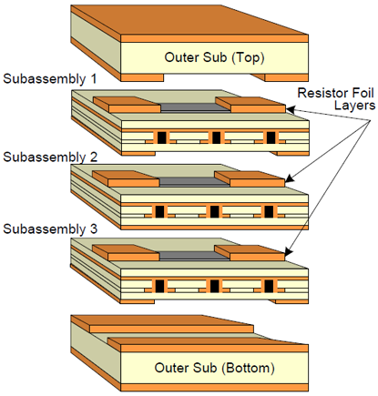 |
1, The embedded resistor layers in multilayer PCBs can be initiated by using cores with a thin film resistor foil laminated to one side instead of the standard copper foil. The specific dielectric properties of the cores may be specified as part of the design or selected by the PCB fabricator to ensure that the electrical requirements of the final product are met. The thin film resistor foil offers excellent peel strength and sheet resistivity values when combined with many commercially available high Tg value, lead-free systems. 2, The inner layers of the subassemblies follow the standard process for creating multilayer printed circuit boards through single lamination. As the resistor layer will be the outermost layer of the subassembly, the lay-up process will commence with the resistor foil either being free-standing or supported. The pre-preg is then applied onto the exposed resistor side of the foil. Care must be taken to avoid sliding the pre-preg over the resistor surface to prevent damage. 3, Once the subassemblies have been laminated together, the resistor elements are no longer exposed. The laminated PCB can then undergo the standard sequence of processes including drilling, plating, imaging, etching, surface finishing, solder masking, routing, and electrical testing. 4, Designing and manufacturing PCBs with embedded resistors, particularly those involving multiple sheet resistivities and multiple layers of buried resistors, can be a challenging task. These processes are further complicated by PCB technologies such as HDI, which commonly coincide with embedded passives. |
Design Considerations of Embedded Resistor PCB : |
Embedded resistor PCBs offer unique advantages in terms of space-saving, improved electrical performance, and enhanced reliability. However, designing such PCBs requires careful consideration of several factors to ensure optimal functionality and manufacturability. 1, Material Selection: |
|
 |
2, Sheet Resistivity Variation: 3, Thermal Management: 4, Signal Integrity: |
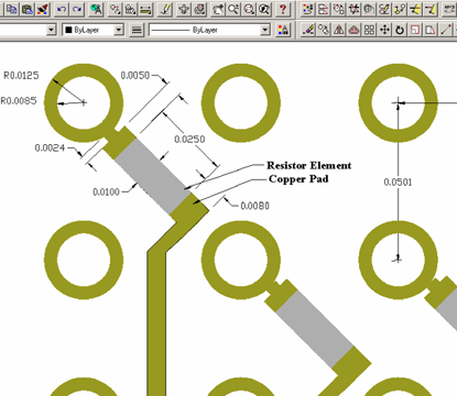
5,Layout and Dimensional Design Rules for Embedded Resistors: 6, Manufacturing Challenges: 7, Testing and Verification: Designing embedded resistor PCBs requires careful consideration of material selection, sheet resistivity variation, thermal management, signal integrity, manufacturing challenges, and testing procedures. By addressing these design considerations, engineers can achieve optimal performance, reliability, and functionality in their embedded resistor PCB designs. |
|
Resistive Foil Specifications of Embedded Resistor PCB : |
Resistive Materials |
NiCr |
NCAS |
CrSiO |
Sheet Resistance (Ω/sq) |
25, 50, 100 |
25, 50, 100, 250 |
1000 |
Sheet Resistivity Tolerance (%) |
±5 |
±5 |
±5 |
Temperature Coefficient of Resistance (ppm/°C) |
<110 |
-20 |
300 |
Base Copper Foil Thickness (microns) |
18, 35 |
18, 35 |
18, 35 |
Width Maximum mm (inches) |
1295 (51) |
1295 (51) |
1295 (51) |
Maximum Recommended Power Dissipation at 40° C (watts/sq in) |
50 Ω /sq: 200 |
50 Ω /sq: 200 |
1000 Ω/sq: 250 |