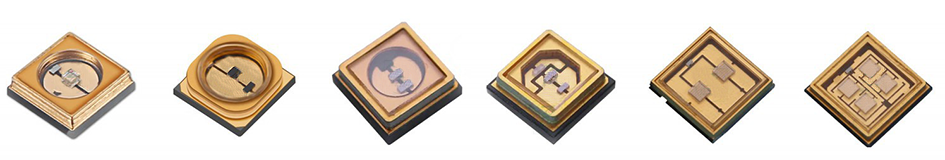
Thin Film Substrates
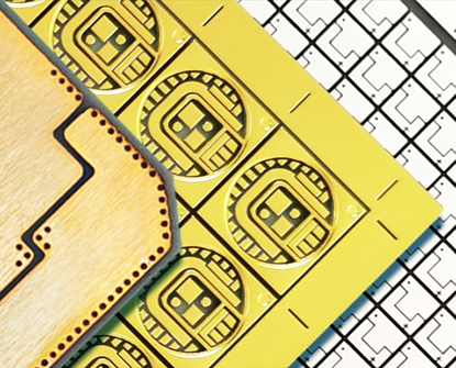
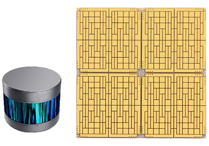
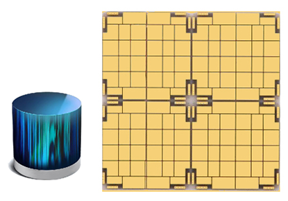
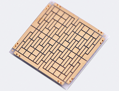
Thin Film Substrates, also known as Thin Film Ceramic Substrates, are advanced materials used to deposit metal thin films, typically copper, onto ceramic substrates through techniques such as physical vapor deposition (PVD), chemical vapor deposition (CVD), direct bonding copper (DBC), direct plate copper (DPC), and active metal brazing (AMB), which utilize vapor-phase deposition to form a uniform and controlled metal layer on the ceramic surface, resulting in a composite material that combines the mechanical robustness of ceramics with the excellent electrical performance of metals. Thin Film Substrates possess several key characteristics that make them highly suitable for precision electronic applications. They offer highly accurate and uniform metal layers, which are essential for the production of precise electronic circuits and components. The ceramic component provides excellent thermal conductivity and mechanical strength, enabling the substrates to function efficiently in high-temperature environments. Additionally, Thin Film Substrates feature a low coefficient of thermal expansion, ensuring stability under varying thermal conditions. Their excellent electrical performance and controllable dimensions make them ideal for miniaturized, high-density circuits. Key Features of Thin Film Substrates : |
 |
|
 |
1, Excellent Electrical Performance 2, Controllable Size and Miniaturization |
|
3, High Precision and Uniformity 4, Excellent Thermal Management |
||
 |
5, High Mechanical Strength and Stability 6, Low Coefficient of Thermal Expansion Thin Film Substrates combine the advantages of ceramic and metal materials, offering excellent thermal management, electrical performance, and mechanical strength. They are widely used in high-frequency electronics, communication devices, LED driver circuits, and other high-performance electronic applications. |
|
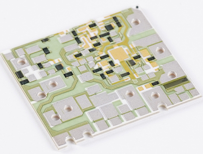
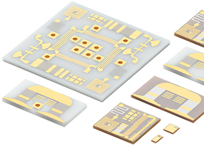
Thin Film Circuit Substrates are widely used in various fields, particularly in high-frequency and high-power electronic devices, such as RF modules, power amplifiers, and high-frequency communication equipment. Due to their exceptional heat management capabilities and superior electrical properties, thin film substrates are also extensively used in demanding industries like aerospace, military electronics, LED driver circuits, and automotive electronics. Furthermore, as electronic products become smaller and more integrated, thin film substrates play an increasingly important role in the development of new electronic devices, particularly in microelectronics and integrated circuit manufacturing. |
||
What Are Thin Film Deposition Technologies ? |
Thin Film Deposition Technologies involve the processes of depositing materials in the form of thin films onto substrates' surfaces. These methods are widely used in the manufacturing of electronic devices, optoelectronic devices, sensors, displays, solar cells, and other high-tech products. These techniques allow precise control over the films' thickness, structure, and composition, enabling them to play key roles in fields such as microelectronics, optoelectronics, energy, and other advanced technologies. Thin Film Deposition Processes involve transforming materials from their solid, liquid, or gas form into a vapor or gas phase, which is then deposited onto the substrate through physical or chemical processes, resulting in thin films with specific properties. The thickness of thin films is typically in the range of nanometers to micrometers, and they can be controlled with high precision and uniformity. Common Thin Film Deposition Techniques include: 1, Chemical Vapor Deposition (CVD) : |
|
 |
2, Physical Vapor Deposition (PVD) : 3, Direct Plasma CVD (DPC) : 4, Direct Bonded Copper (DBC) : |
5, Active Metal Brazing (AMB) : 6, Other Thin Film Deposition Techniques : ● Atomic Layer Deposition (ALD): A high-precision thin-film deposition technique that allows for atomic-scale control of film thickness. ALD is widely used in nanotechnology and semiconductor manufacturing. ● Molecular Beam Epitaxy (MBE): A method where thin films are grown on a substrate in an ultra-high vacuum environment using molecular beams. It is commonly used for the growth of high-quality semiconductor thin films. Thin Film Deposition Techniques are crucial in modern electronics, optoelectronics, energy, and other industrial fields. They enable the production of high-performance, precisely controlled thin films that meet the increasing demands for miniaturization and enhanced performance. |
|
Applications of Thin Film Ceramic Substrates : |
Thin Film Ceramic Substrates are important materials in the electronics field, widely used in various high-end electronic products, especially in environments that require high performance, high reliability, and high temperature or high-frequency operations. The thin-film structures of ceramic substrates provide superior performance compared to traditional metal substrates, making them critical in many applications. Below are some of the primary uses of thin film ceramic substrates: 1. High-Frequency and High-Power Devices : ● High-Power Devices: The good thermal conductivity of ceramic substrates makes them especially suitable for high-power electronic devices like power amplifiers and lasers, where they can effectively dissipate heat and prevent overheating, thus ensuring stable device performance. |
|
 |
2. Semiconductor Packaging : ● Optoelectronic Device Packaging: Thin Film Ceramic Substrates are also used in the packaging of optoelectronic devices such as LEDs and laser diodes. 3. Automotive Electronics : |
● Electric Vehicle (EV) Systems: Thin Film Ceramic Substrates are also used in electric vehicle systems, including battery management systems, charging systems, and electric motor drives. These devices require stable operation under high power density and heat load conditions, where ceramic substrates excel. 4. Optics and Laser Technology : ● Optical Devices: Thin Film Ceramic Substrates are also used in optical devices, such as optical sensors and interferometers, where their stability and precision make them ideal for improving the performance and accuracy of optical systems. |
|
 |
5. Military and Aerospace : ● Aerospace: In aerospace applications, ceramic substrates are used in flight control systems, navigation devices, and other critical components. These systems often need to operate under extreme temperature fluctuations and high vibrations, making ceramic substrates essential for providing reliability and stability. 6. Medical Electronics : |
● Implantable Devices: Thin Film Ceramic Substrates are used in various implantable medical devices such as pacemakers and neural stimulators. Their biocompatibility and stability make them suitable for long-term use within the human body. 7. Energy and Environmental Applications : ● Environmental Monitoring Equipment: Thin Film Ceramic Substrates are used in environmental monitoring devices like gas sensors and air quality monitoring equipment. Their chemical stability and corrosion resistance make them perform well in harsh environmental conditions. Thin Film Ceramic Substrates offer unique performance advantages, especially in terms of high temperature, high frequency, high power, stability, and durability, making them critical materials in many high-end applications across electronics, optoelectronics, automotive, military, medical, and other fields. As technology advances and the demand for more sophisticated applications grows, the use of ceramic substrates is expected to expand further, especially in electronics that require higher precision, higher power, and more complex designs, where ceramic substrates will continue to demonstrate their value. |
|
Thick Film Substrates VS Thin Film Substrates : |
Thick Film Substrates and Thin Film Substrates are commonly used materials in electronic manufacturing, each having distinct characteristics, advantages, and applications. Below are the main differences between these two types of ceramic substrates, along with their respective pros and cons. 1. Manufacturing Process Differences : ● Thin Film Substrates: The thin-film technology involves depositing very thin layers of metal, insulator, or other materials onto the ceramic substrate through techniques such as chemical vapor deposition (CVD) or physical vapor deposition (PVD). The film thickness is typically under a few microns, and the process is more precise, requiring more advanced technology. |
|
 |
2. Electrical Performance : ● Thin Film Substrates: Thin-film substrates usually offer superior electrical characteristics, including low capacitance and low loss, which makes them ideal for high-frequency applications. They also have better insulation and electrical stability. 3. Thermal Performance : |
● Thin Film Substrates: Thin-film substrates generally have better thermal stability, and because of their thinner film layers, they offer higher thermal conductivity. This makes them better suited for applications requiring rapid heat dissipation and high-performance electronic components. 4. Mechanical Performance : ● Thin Film Substrates: Thin-film substrates, due to their thinner layers, have relatively weaker mechanical strength and are more prone to cracking or delamination. As a result, special care must be taken in the design and handling of these substrates. 5. Application Fields : |
|
 |
● Thin Film Substrates: Thin-film substrates are widely used in high-frequency, high-power, and precision electronic devices, such as microwave communications, satellite communications, laser systems, and high-speed computer circuits. They are ideal for high-end electronic devices that demand precise dimensions, high performance, and signal integrity. 6. Manufacturing Costs : ● Thin Film Substrates: Thin-film technology involves more complex deposition processes and fine fabrication techniques, resulting in higher manufacturing costs. These substrates are typically used in high-end, precision applications where performance outweighs cost considerations. |
7. Pros and Cons Summary : ● Cons: Inferior electrical performance; poor thermal performance; less precision, not ideal for high-frequency or high-precision applications. Thin Film Substrates: ● Cons: Higher cost, suitable for high-end markets; weaker mechanical strength, requiring additional protection; more complex production process, not ideal for large-scale, low-cost manufacturing. Thick Film Substrates and Thin Film Substrates each have unique advantages and drawbacks. Thick-film substrates are better suited for low-cost, large-scale electronic applications, while thin-film substrates are essential for high-performance, precision electronic devices. The choice of substrate material depends on the specific requirements of the application, such as electrical performance, thermal management, mechanical durability, and production cost. |
|
Manufacturing Challenges of Thin Film Ceramic Substrates : |
Thin Film Ceramic Substrates are manufactured through a process that involves several technical challenges, primarily including material selection, thin film deposition techniques, thickness uniformity control, sintering processes, and cost management. Below is a detailed description of these challenges: 1. Material Selection : |
|
 |
2. Thin Film Deposition Techniques : ● Sputtering: The sputtering power, gas atmosphere, temperature, and other factors must be carefully controlled to ensure the quality and uniformity of the thin film. ● CVD: This process requires strict control of gas flow, temperature, and pressure to ensure the density and consistency of the thin film's chemical composition. Different deposition methods and process conditions directly affect the thin film's microstructure, surface smoothness, and functionality (such as conductivity or insulation), making process optimization extremely important. |
3. Thickness and Uniformity Control : Common solutions include adjusting deposition rates, optimizing process parameters, and using multi-layer deposition techniques to improve thin film uniformity. 4. Sintering Process : During sintering, high temperatures can lead to substrate deformation or cracking, particularly when there is a mismatch between the thermal expansion coefficients of the substrate and the thin film. To prevent cracking and deformation, it is necessary to optimize the thermal expansion coefficients of the materials and carefully control the sintering temperature and time. |
|
 |
5. Surface Treatment and Functionalization : 6. Final Product Inspection and Testing : ● Electrical Testing: This involves testing the substrate’s conductivity, dielectric constant, and insulation properties. ● Mechanical Testing: Includes hardness, bending strength, tensile strength. |
● Thermal Testing: Such as thermal conductivity and thermal expansion coefficient. These tests require extremely high precision and consistency, as even minor deviations can affect the final product quality. 7. Cost Management : Thin Film Ceramic Substrates are complex and highly demanding materials to manufacture, involving several key processes such as material selection, thin film deposition, sintering, surface treatment, and more, with precise control at each step being crucial to ensuring the quality and performance of the final product, making addressing these technical challenges essential for achieving high-quality and cost-effective production in the industry. |
|
Design Guidelines of Thin Film Substrates : |
We compiled a Thin Film Substrates-Design Guidelines as attached for you to download, It is to better support our customers' needs in designing and applying Thin Film Substrates, This guide covers detailed information on product solutions, engineering design specifications, material properties, available manufacturing processes, and more. We hope that this guide will assist customers in standardizing their design process while ensuring the manufacturability of the design data, ultimately improving product reliability and production efficiency. Customers are encouraged to refer to the guide when designing Thin Film Substrates to ensure adherence to best practices. |
Optional Materials of Thin Film Substrates : |
Substrates : |
Alumina (Al2O3) |
Aluminum Nitride (AlN) |
Beryllium Oxide (BeO) |
Zirconium Dioxide (ZrO2) |
Max Application Temperature : |
662 - 1832 |
1832 |
2300 |
2432 |
Max Power Density (W/in²): |
75 |
1010 |
250 |
300 |
Max Ramp Up Speed (°F/sec): |
122 |
572 |
400 |
350 |
Thermal Conductivity (W/mK): |
20-35 |
180-220 |
200-300 |
2.0-5.0 |
Density (g/cm³): |
3.75 |
3.26 |
2.8 |
5.9 |
Dielectric Loss: |
0.0001 - 0.001 |
0.0001 - 0.0005 |
0.0001 - 0.0002 |
0.0005 - 0.001 |
Dielectric Constant: |
9.4 - 10.2 |
8.5 - 9.0 |
6.0 - 7.0 |
25 - 30 |
CTE, ppm/ºC: |
6.0 - 8.0 |
4.0 - 5.0 |
7.0 - 9.0 |
10.0 - 11.0 |
Substrate Thickness (mm): |
0.25 - 2.0 |
0.25 - 2.0 |
0.25 - 2.0 |
0.25 - 2.0 |
Typical Max. Dimension (inch): |
6 x 12 |
5 x 11 |
6 x 6 |
4 x 4 |
Theoretical Total Wattage (W): |
5400 |
55000 |
15000 |
20000 |
Optional Processes of Thick Film and Thin Film Substrates : |
Metalization Types : |
Thick Film Substrates (Screen-Printed) |
Thin Film Substrates (Photo-Imaged) |
|||
Process Types : |
TFM Capabilities |
HTCC / LTCC Capabilities |
DBC Capabilities |
DPC Capabilities |
AMB Capabilities |
Layer Counts : |
1, 2, 3, 4, 5, 6 Layers |
1, 2, 4, 6, 8, 10, 12 Layers |
1, 2 Layers |
1, 2 Layers |
1, 2 Layers |
Max Board Dimension : |
200*230mm |
200*200mm |
138*178mm |
138*190mm |
114*114mm |
Min Board Thickness : |
0.25mm |
0.25mm |
0.30mm~0.40mm |
0.25mm |
0.25mm |
Max Board Thickness : |
2.2mm |
2.0mm |
1L: 1.6mm; 2L 2.0mm |
2.0mm |
1.8mm |
Conductor Thickness : |
10um - 20um |
5um - 1500um |
1oz - 9oz |
1um - 1000um |
1oz- 22oz |
Min Line Width/Space : |
8/8mil (0.20/0.20mm) |
6/6mil (0.15/0.15mm) |
10/10mil (0.25/0.25mm) |
6/6mil (0.15/0.15mm) |
12/12mil (0.30/0.30mm) |
Substrates Types : |
AI203, ALN, BeO, ZrO2 |
AI203, ALN, BeO, ZrO2 |
Al2O3, AlN, ZrO2, PbO, SiO2, ZTA, Si3N4, SiC, Sapphire, Polycrystalline Silicon, Piezoelectric Ceramics |
Al2O3, AlN, ZrO2, PbO, SiO2, ZTA, Si3N4, SiC, Sapphire, Polycrystalline Silicon, Piezoelectric Ceramics |
AI203, ALN, BeO, ZrO2, Si3N4 |
Min Hole Diameter : |
4mil (0.15mm) |
4mil (0.15mm) |
4mil (0.1mm) |
4mil (0.1mm) |
4mil (0.1mm) |
Outline Tolerance : |
Laser: +/-0.05mm; Die Punch: +/-0.10mm |
Laser: +/-0.05mm; Die Punch: +/-0.10mm |
Laser: +/-0.05mm; Die Punch: +/-0.10mm |
Laser: +/-0.05mm; Die Punch: +/-0.10mm |
Laser: +/-0.05mm; Die Punch: +/-0.10mm |
Substrate Thickness : |
0.25, 0.38, 0.50, 0.635, 0.80,1.0, 1.25, 1.5, 2.0mm, Customizable |
0.25, 0.38, 0.50, 0.635, 0.80,1.0, 1.25, 1.5, 2.0mm, Customizable |
0.25, 0.38, 0.50, 0.635, 0.80,1.0, 1.25, 1.5, 2.0mm, Customizable |
0.25, 0.38, 0.50, 0.635, 0.80,1.0, 1.25, 1.5, 2.0mm, Customizable |
0.25, 0.38, 0.50, 0.635, 0.80,1.0, 1.25, 1.5, 2.0mm, Customizable |
Thickness Tolerance : |
0.25-0.38: +/-0.03mm; 0.50-2.00: +/-0.05mm |
0.25-0.38: +/-0.03mm; 0.50-2.00: +/-0.05mm |
0.25-0.38: +/-0.03mm; 0.50-2.00: +/-0.05mm |
0.25-0.38: +/-0.03mm; 0.50-2.00: +/-0.05mm |
0.25-0.38: +/-0.03mm; 0.50-2.00: +/-0.05mm |
Surface Treatment : |
Ag, Au, AgPd, AuPd |
Ag, Au, AgPd, AuPd, Mn/Ni |
OSP/Ni Plating, ENIG |
OSP/ENIG/ENEPIG |
OSP/ENIG/ENEPIG |
Min Solder PAD Dia : |
10mil (0.25mm) |
10mil (0.25mm) |
8mil (0.20mm) |
6mil (0.15mm) |
8mil (0.20mm) |