PCB Design Services
PCB Design Services, also known as PCB Layout Services, are comprehensive processes of designing Printed Circuit Boards, involving collaborations across various disciplines such as electrical engineering, mechanical engineering, and design principles, with key tasks including the precise placements of components and meticulous routings of electrical connections to ensure optimal functionalities, adherence to design specifications, and overall performance requirements. PCB Design Services cover the entire project lifecycle, from initial concept to final manufacturing. These services involve electrical analysis, component selection, and schematic creation. Engineers ensure the design can handle electrical signals efficiently while addressing thermal management to prevent overheating and ensure reliability. PCB Layout Services also focus on the mechanical and aesthetic aspects of the board. This includes optimizing component placement, size reduction, and ensuring manufacturability. Designers use simulation tools to test performance and ensure compliance with industry standards and enhancing overall product quality. |
 |
PCB Design Services are to create an efficient, reliable, and cost-effective design for the specific requirements of the project. This can be a complex task due to the many factors that need to be considered, such as the physical constraints of the board, the electrical requirements of the circuit, and the needs of the manufacturing process. |
|
Key Features and Aspects of PCB Design Services : |
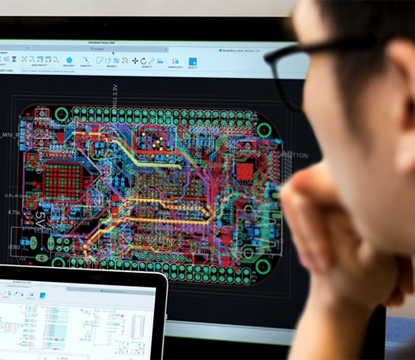
PCB Design encompasses numerous features and considerations that are crucial for the successful creation of a functional and reliable printed circuit board. Here are some key features and aspects of PCB design: 1, Layer Stack-up: Modern PCBs can have multiple layers, including signal, power, and ground planes. The stack-up configuration is vital for signal integrity, impedance control, and electromagnetic compatibility (EMC). 2, Component Placement: Strategic placement of components is critical to minimize signal path lengths, reduce noise, and manage heat. Components must also be placed to facilitate manufacturability and testing. 3, Routing: This involves creating paths for electrical signals between components. Effective routing minimizes cross-talk and signal degradation while adhering to design rules such as trace width, spacing, and impedance requirements. 4, Signal Integrity: High-speed designs require careful consideration of trace geometry, board materials, and routing techniques to ensure signals are transmitted without significant loss or distortion. |
|
 |
5, Power Integrity: Adequate power distribution must be ensured with proper planning of power planes, voltage regulators, decoupling capacitors, and power filtering to maintain stable and clean power supply. 6, Thermal Management: Heat dissipation is addressed through the use of heat sinks, thermal vias, and careful component placement to prevent hot spots and ensure the longevity of the board. 7, Design for Manufacturability (DFM): The design must account for the capabilities and limitations of PCB manufacturing processes to avoid production issues and reduce costs. 8, Design for Testing (DFT): Test points and strategies should be incorporated into the design to enable efficient testing of the PCB during production and troubleshooting. 9, Grounding and Shielding: Proper grounding techniques and the use of shielding can mitigate interference and improve the EMC performance of the PCB. |
10, Via Types: The design may include various types of vias, such as through-hole, blind, or buried vias, depending on the complexity of the board and the interconnection needs. 11, Gerber Files and Documentation: Comprehensive documentation, including Gerber files, assembly drawings, and bills of materials (BOM), is generated to guide the manufacturing and assembly process. 12, Mechanical Constraints: The PCB design must consider the mechanical enclosure and mounting requirements, ensuring that the board fits within the intended space and aligns with connectors and other mechanical components. 13, Regulatory Compliance: The design must comply with industry standards and regulations, such as IPC standards, UL certification, FCC guidelines for EMC, etc. 14, Revision Control: Keeping track of design revisions and maintaining a history of changes is important for future updates and troubleshooting. 15, Simulation and Analysis: Before prototyping, simulations like SPICE for circuit behavior, thermal analysis, and signal integrity analysis can predict performance and identify potential issues. A well-designed PCB not only ensures the functionality of the electronic device but also its reliability, manufacturability, and cost-effectiveness. PCB designers use specialized software tools to integrate these features into a cohesive design that meets all the specified requirements. |
|
Why Choose PANDA PCB for PCB Layout Services : |
PANDA PCB Group offers comprehensive PCB Layout Services to our customers. Our team comprises over 25 professional PCB engineers, each with extensive design experience, they are well-versed in tackling complex PCB designs and can navigate the intricacies of various design types, ensuring high-quality outcomes. We operate under a complete workflow system and utilize independently developed software to enhance design efficiency. 1, Advanced Tools and Software: We employ state-of-the-art, independently developed software, which allows us to enhance design efficiency and accuracy. This investment in technology translates to faster turnaround times and more reliable designs for our customers. 2, Versatility in Design: Our capabilities include a broad spectrum of PCB design types, from high-density interconnect (HDI) boards to high-speed backplanes. No matter the complexity, we can handle designs with up to 40 layers, catering to a wide range of industry needs. |
|
 |
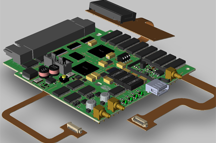
3, Cutting-Edge Design Products: Panda PCB stays at the forefront of technology by working with advanced components and design requirements. Our portfolio includes designs with high-speed interfaces like PCI-EXPRESS and SATA, as well as experience with leading-edge technologies such as ARM series processors and high-speed signal design and simulation. 4, Layout Solution: Customers are required to provide us with schematics, Netlists, structural diagrams, datasheets, specifications, etc. Upon completion of the design, we will provide the customer with the PCB Gerber file, assembly files, stencil files, and updated structural diagrams. 5, PCB Design Types: We specialize in a wide range of PCB designs including high frequency, high speed, high-density, high-voltage, high-power, RF, backplane, ATE, flexible board, rigid-flexible board, and aluminum substrate designs. We can handle complex designs of up to 40 layers. |
6, PCB Design Products: Our design expertise spans various sectors such as Industrial Control, Radar Communications, Computers, Digital Consumer Electronics, Instrumentation, Video Equipment, and Electrical Energy. For instance, we have experience working with PCI- EXPRESS, SATA & SATAII, Virtex-7 Spartan-6 TI DSP series, BCM5696 BCM56601, DDR & DDRII, MX630 FX930, ARM7 & ARM 9 series, programmable logic, DLP-RAMBUS RLDRAM, switch power supply, and high-speed backplanes with 25Gbps+ signal design and simulation capabilities. 7, Quality Assurance and Compliance: We adhere to strict quality control measures and comply with international standards, ensuring that every design meets or exceeds the required specifications and regulations. 8, Comprehensive Service Offering: Panda PCB provides an all-encompassing service that includes everything from initial layout solutions to the delivery of manufacturing-ready files. Customers receive detailed documentation, including PCB Gerber files, assembly files, and stencil files, ensuring a smooth transition to production. |
|
Capabilities of PCB Design Services : |
 |
|
Basics Terminologies of PCB Layout Services : |
|
Deliverables of PCB Design Services : |
|
 |
Delivery Time of PCB Design Services : |
Feedback Review of PCB Design : |
||||||||||||||||||||
|
1, Once job is start, we will check the requirements with all relevant details and manufacturing guidelines,after that we can provide customer the components placement drawing in PDF format.Then It is customer's responsibility to review that the component placements and its foot prints are acceptable. After we got the confirmation form customer, we will update the component layout and complete the routing path. The routing documents is sent as PDF documents with Gerber files again. Customer should approve the PCB design based on the documents sent or request an online review at that stage. |