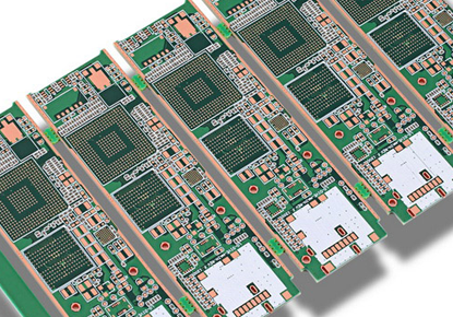
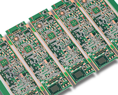
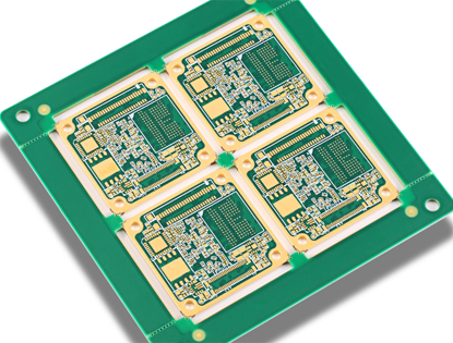
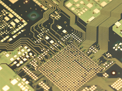
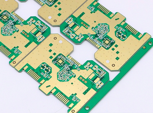
Halogen-Free PCB
Halogen-Free PCBs refer to special printed circuit boards that do not contain halogen elements such as fluorine, chlorine, bromine, or iodine. whereas traditional PCB materials often contain halogens in the form of flame-retardant additives, which can produce toxic gases when exposed to high temperatures, such as during a fire or improper disposal. Halogen-Free PCBs are defined by the IPC 4101B standard in the electronics industry, which specifies that bromine levels must be below 900 PPM by weight, chlorine levels must be below 900 PPM by weight, and the combined weight of bromine and chlorine must be below 1500 PPM. Halogen-Free PCBs, in accordance with the IEC 61249-2-21 and JPCA-ES-01-2003 standards, are printed circuit boards with copper cladding that contain chlorine and bromine at or below 0.09 wt% (900ppm), with the total halogen content not exceeding 0.15 wt% (1500ppm). These environmentally friendly PCBs reduce the risk of toxic emissions during high-temperature events, such as fires or improper disposal. Commonly used in industries like automotive, telecommunications, and consumer electronics, they help minimize the environmental impact of electronic waste and meet global regulations for safe disposal. Development Prospect of Halogen- Free PCB : |
 |
|
 |
1, Halogen-Free PCB Development: Concerns about the health and safety risks associated with halogenated flame retardants in printed wiring board (PWB) applications have been raised since the early 1990s. It was discovered that brominated flame retardants used in PWBs could lead to the release of highly toxic dioxins and furans during combustion, especially when incomplete. While halogenated materials may offer cost advantages in some applications by providing necessary performance characteristics, the shift towards using Halogen-Free PCB materials is driven by the growing urgency of environmental protection. 2, Although legislation does not currently mandate the removal of brominated and chlorinated flame retardants from electronic component PCB materials, the increasing demand for environmental responsibility is leading more electronic products to adopt halogen-free PCBs, which are both safer for health and more recyclable. |
|
3, While the use of Halogen-Free PCBs signifies a step towards enhancing safety, health, and environmental friendliness in certain applications, it is important to note that it does not guarantee overall product superiority in these aspects. When it comes to fire safety, the term "halogen-free" specifically relates to the reduced toxicity of smoke emissions during material combustion. Halogen-free products are designed to minimize the release of toxic or corrosive gases when ignited, thus contributing to a safer environment. In contrast, certain types of halogenated PCB materials not only pose risks to human health and animals but also have adverse effects on the environment. |
||
Key Features of Halogen-Free PCB : |
1, Environmental Safety: Halogen-Free PCBs eliminate the use of brominated and chlorinated flame retardants, reducing the release of toxic substances during combustion and minimizing environmental impact. This makes them a more environmentally friendly choice compared to traditional halogenated PCBs. 2, Health Benefits: By removing halogen compounds from PCB materials, Halogen-Free PCBs contribute to a safer working environment for manufacturing and end-users. They reduce the risk of exposure to harmful chemicals and promote better health outcomes for individuals handling electronic products. |
|
 |
3, Compliance with Regulations: Halogen-Free PCBs meet international standards and regulations for environmental protection and product safety. Their composition aligns with restrictions on hazardous substances, ensuring compliance with laws such as RoHS (Restriction of Hazardous Substances Directive). 4, Improved Recycling Potential: The absence of halogens in Halogen-Free PCBs facilitates easier and more efficient recycling processes. This supports circular economy principles by promoting the reuse of electronic components and reducing electronic waste. 5, Enhanced Fire Safety: Halogen-Free PCBs are designed to emit lower levels of toxic gases and smoke when exposed to fire, improving overall fire safety in electronic devices and applications. This feature enhances workplace and consumer safety in the event of a fire incident. |
6, Reliability and Performance: Despite the removal of halogen compounds, Halogen-Free PCBs maintain high performance standards and reliability levels. They offer consistent electrical properties, thermal stability, and mechanical strength, meeting the requirements of modern electronic applications. 7, Future-Proof Design: The adoption of Halogen-Free PCBs positions manufacturers and designers for future regulatory changes and market demands. As sustainability becomes increasingly important in the electronics industry, Halogen-Free PCBs ensure a forward-thinking approach to product development. |
|
Applications of Halogen-Free PCB : |
Halogen-Free PCBs find applications in a wide range of electronic devices and systems where environmental friendliness, safety, and regulatory compliance are key considerations. Some common applications include: 1, Consumer Electronics: Halogen-Free PCBs are widely used in consumer electronic devices such as smartphones, tablets, laptops, digital cameras, and smart home appliances. These products often come into close contact with users, making the absence of halogens an important factor in promoting user safety and environmental responsibility. 2, Automotive Electronics: With the increasing electrification of vehicles, including electric and hybrid cars, the demand for Halogen-Free PCBs in automotive electronics has risen. These PCBs are used in various control units, infotainment systems, sensors, and other electronic components within vehicles, contributing to improved safety and sustainability in the automotive sector. |
|
 |
3, Industrial Equipment: Halogen-Free PCBs are utilized in industrial equipment such as automation systems, control panels, instrumentation, and manufacturing machinery. The use of halogen-free materials aligns with industry standards for safety, reliability, and environmental compliance in industrial settings. 4, Medical Devices: In the healthcare sector, medical devices and diagnostic equipment often incorporate Halogen-Free PCBs to ensure the highest levels of safety and biocompatibility. These PCBs are critical in applications such as patient monitoring systems, imaging devices, laboratory equipment, and medical instrumentation. 5, Aerospace and Defense: The aerospace and defense industries rely on electronic systems that meet stringent safety and reliability standards. Halogen-Free PCBs are employed in avionics, communication systems, radar equipment, and military electronics, where compliance with environmental regulations and reduced fire hazards are essential. |
6, Telecommunications: In telecommunications infrastructure and networking equipment, Halogen-Free PCBs are used to support reliable and high-performance communication systems. These PCBs are crucial in applications ranging from base stations and routers to fiber optic transmission equipment. 7, Renewable Energy Systems: Solar inverters, wind turbine control systems, and energy storage devices utilize Halogen-Free PCBs to ensure the safety and sustainability of renewable energy generation and distribution technologies. The use of Halogen-Free PCBs spans diverse industries and applications, reflecting the growing emphasis on environmental responsibility, safety, and regulatory compliance across the electronic manufacturing landscape. |
|
Design Considerations of Halogen-Free PCB : |
When designing Halogen-Free PCBs, several key considerations should be taken into account to ensure optimal performance, reliability, and compliance with environmental regulations. Here are some design considerations for Halogen-Free PCBs: 1, Material Selection: Choose halogen-free materials for the substrate, laminate, solder mask, and surface finish of the PCB. Ensure that all materials used in the PCB construction are free from brominated and chlorinated compounds to meet halogen-free requirements. 2, Flame Retardancy: Select flame-retardant materials that do not contain halogens but still provide adequate fire resistance properties. Consider using alternative flame retardants such as phosphorus-based compounds to achieve the desired level of fire safety without compromising environmental friendliness. |
|
 |
3, Thermal Management: Pay attention to thermal management considerations to ensure efficient heat dissipation and temperature control on the PCB. Proper heat dissipation is essential for maintaining the reliability and performance of electronic components, especially in applications with high power density. 4, Signal Integrity: Optimize the layout and routing of signal traces to minimize signal interference, crosstalk, and impedance mismatch. Follow best practices for signal integrity design, including controlled impedance routing, signal grounding, and signal isolation to maintain signal quality and reliability. 5, EMI/EMC Compliance: Design the PCB layout and stackup to mitigate electromagnetic interference (EMI) and ensure electromagnetic compatibility (EMC). Use proper shielding techniques, ground planes, and signal isolation to reduce EMI emissions and susceptibility to external interference. 6, Component Placement: Carefully position components on the PCB to optimize signal paths, reduce signal distortion, and improve thermal performance. Consider factors such as component density, signal integrity requirements, thermal coupling, and accessibility for assembly and maintenance. |
7, Environmental Impact: Consider the environmental impact of the PCB design throughout its lifecycle, from manufacturing and use to disposal or recycling. Choose materials and manufacturing processes that minimize waste, energy consumption, and greenhouse gas emissions to promote sustainability and eco-friendliness. 8, Compliance with Regulations: Ensure that the Halogen-Free PCB design meets relevant regulations and standards, such as RoHS, REACH, and IEC 61249-2-21, governing the use of hazardous substances in electronic products. Verify the compliance of materials, processes, and the final product to avoid regulatory non-compliance issues. By incorporating these design considerations into the development of Halogen-Free PCBs, manufacturers can create environmentally friendly, safe, and high-performance printed circuit boards that meet the evolving needs of the electronics industry while promoting sustainability and regulatory compliance. |
|
Manufacturing Challenges of Halogen-Free PCB : |
Manufacturing Halogen-Free PCBs presents several challenges that manufacturers need to address to ensure the quality, reliability, and cost-effectiveness of the printed circuit boards. Some of the key manufacturing challenges associated with Halogen-Free PCBs include: 1, Material Availability: One of the primary challenges in manufacturing Halogen-Free PCBs is the availability of suitable halogen-free materials for substrate, laminate, solder mask, and surface finish. While halogen-free alternatives are becoming more common, manufacturers may face limitations in material options and suppliers compared to traditional halogen-containing materials. 2, Compatibility with Processes: Halogen-Free materials may have different properties and behaviors during the manufacturing processes, such as etching, plating, soldering, and assembly. Manufacturers need to ensure that these materials are compatible with existing processes and equipment to maintain production efficiency and product quality. |
|
 |
3, Thermal Management: Halogen-Free PCBs may have different thermal properties compared to traditional PCBs containing halogens. Managing heat dissipation, thermal expansion, and thermal stress becomes crucial to prevent issues such as delamination, warping, or component damage during manufacturing and operation. 4, Cost Considerations: The cost of Halogen-Free materials and manufacturing processes may be higher than traditional halogen-containing materials, impacting the overall production costs of PCBs. Manufacturers need to balance the benefits of environmental friendliness and regulatory compliance with cost-effectiveness to remain competitive in the market. 5, Process Optimization: Adapting manufacturing processes to accommodate the characteristics of Halogen-Free materials requires process optimization and parameter adjustments. Manufacturers may need to fine-tune processes such as soldering, reflow, lamination, and cleaning to achieve the desired quality and reliability in Halogen-Free PCB production. |
6, Testing and Quality Assurance: Ensuring the quality and reliability of Halogen-Free PCBs through testing and quality assurance processes is essential. Manufacturers need to validate the performance, durability, and compliance of the PCBs using appropriate testing methods and standards to meet customer requirements and regulatory specifications. 7, Supply Chain Management: Managing the supply chain for Halogen-Free materials and components is critical to maintaining production continuity and product consistency. Manufacturers need to work closely with suppliers to ensure a reliable source of materials and components that meet quality and environmental standards. By addressing these manufacturing challenges effectively and implementing best practices in material selection, process optimization, quality control, and supply chain management, manufacturers can successfully produce high-quality, environmentally friendly Halogen-Free PCBs that meet industry standards and customer expectations. |
|
Advantages of Halogen-Free PCB : |
1, Improved Electrical Insulation: Halogen-free PCBs exhibit better electrical insulation properties due to the reduced polarity resulting from the use of nitrogen and phosphorus instead of halogens. This lower polarity allows halogen-free PCBs to withstand higher electric shocks effectively. 2, Lower Thermal Coefficient: By incorporating phosphorus and nitrogen in place of halogens, halogen-free PCBs possess a higher molecular weight, leading to increased thermal stability and reduced thermal expansion compared to traditional epoxy resin-based PCBs. This improved thermal stability is crucial for maintaining performance under varying temperature conditions. |
|
 |
3, Reduced Moisture Absorption: Epoxy resins containing phosphorus and nitrogen have a lower tendency to form hydrogen bonds with water molecules, resulting in lower moisture absorption rates for halogen-free PCBs. In contrast, halogen-containing PCBs are more prone to moisture absorption due to hydrogen bonding, making halogen-free PCBs more reliable in humid environments. 4, Lower Toxicity: Halogen-free PCBs present reduced health risks to technicians and users compared to PCBs containing halogens, as they do not release toxic halogen gases when exposed to high temperatures. This makes halogen-free PCBs a safer choice for both manufacturing and end-use applications. 5, Environmental Friendliness: Halogen-free circuit boards contribute to environmental sustainability by posing fewer risks to the environment. Their lower halogen content makes disposal easier and less harmful to ecosystems, especially in areas where PCB recycling facilities are limited. |
6, Cost-Effective Solution: Halogen-free PCBs offer a cost-effective option for applications requiring single-use electronics, balancing performance and environmental considerations with affordability. 7, Enhanced PCB Properties: Halogen-free PCBs demonstrate properties that are favorable for assemblers, including lower coefficient of thermal expansion (CTE), longer T-260 and T-288 times, and higher decomposition temperature (Td). These characteristics make halogen-free PCBs well-suited for multiple reflow processes and capable of withstanding higher reflow temperatures during PCBA, ensuring reliability and durability in electronic assemblies. By leveraging these advantages, manufacturers can produce high-quality, environmentally friendly, and reliable Halogen-Free PCBs that meet the evolving demands of the electronics industry. |
|
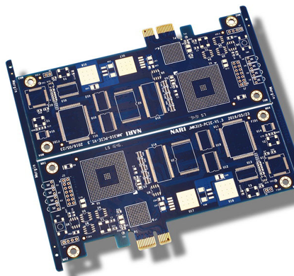
What Are Materials Used For Halogen-Free PCB ? |
1, Substrate Material: The substrate material forms the base of the PCB and is typically made of fiberglass-reinforced epoxy resin, though alternatives such as polyimide or other thermoset materials may also be used. These materials provide the mechanical support and electrical insulation for the PCB. Halogen-Free PCB based on FR4 materials include but are not limited to Panasonic's R1566, R1566WN, R1566W, R1566S, Ventec's VT-447, ITEQ's IT-170GRA1TC, Isola's DE156 and GreenSpeed series, ShengYi's S1550G, S1165, S1165M, S6015. 2, Copper Foil: Copper foil is used to create the conductive traces and pads on the PCB. It is laminated onto the substrate material and then etched to form the desired circuit pattern. |
|
 |
3, Laminate Material: The laminate material provides the insulating layers between copper traces and is typically made of glass fiber cloth impregnated with epoxy resin. However, for Halogen-Free PCBs, alternative materials such as PTFE (Polytetrafluoroethylene) or FR-4 (Flame Retardant 4) with halogen-free flame retardants may be used. 4, Solder Mask: Solder mask is a protective layer applied over the copper traces to prevent unintended solder bridging during assembly. Halogen-Free PCBs use solder mask materials that are free from halogenated compounds. 5, Surface Finish: The surface finish is applied to the exposed copper pads to protect them from oxidation and facilitate soldering during assembly. Common surface finish options for Halogen-Free PCBs include lead-free HASL (Hot Air Solder Leveling), ENIG (Electroless Nickel Immersion Gold), or OSP (Organic Solderability Preservatives) that comply with halogen-free requirements. |
6, Conductive Paste: For PCBs with embedded components or vias, conductive pastes are used to create the conductive pathways. These pastes are formulated with halogen-free materials to ensure compliance with environmental regulations. 7, Additives and Fillers: Various additives and fillers may be incorporated into the raw materials to enhance specific properties of the PCB, such as flame retardancy, thermal conductivity, or dimensional stability. In the case of Halogen-Free PCBs, these additives and fillers are carefully selected to ensure compliance with halogen-free standards. |
|
Why Were Halogen-Free PCB Created ? |
1, Although halogens play essential roles in PCB construction, they have one drawback that’s hard to overlook: toxicity. Chlorine and bromine are the main culprits here. Exposure to either of these chemicals can provoke unpleasant symptoms like nausea, coughing, skin irritation, and blurry vision. Dangerous exposure isn’t likely to occur through handling a PCB that contains halogens. Still, if the PCB catches fire and emits fumes, you can anticipate these adverse side effects. 2, If chlorine-containing components happen to mix with hydrocarbons, the result is dioxin, a lethal carcinogen. Unfortunately, certain countries tend to practice poor disposal due to limited resources to recycle PCBs safely. For this reason, improper disposal of PCBs containing high quantities of chlorine is dangerous for the ecosystem. Burning these gadgets to get rid of them, which does happen, can release dioxin into the environment. To qualify as a halogen-free PCB, a circuit board must not contain more than a certain quantity of halogens. |
 |