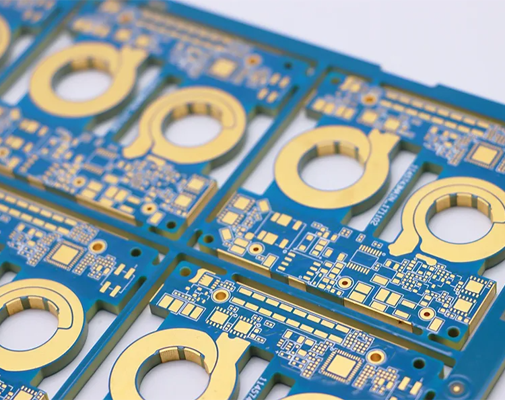
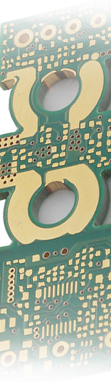
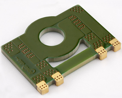
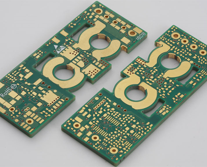
Heavy Copper PCB
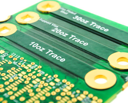
Heavy Copper PCBs, also known as Power Supply PCBs, are special printed circuit boards with a higher copper weight than standard PCBs, typically ranging from 3oz to 12oz or more, providing enhanced current-carrying capacity and heat dissipation for demanding applications such as power supplies, automotive systems, and industrial equipment, capable of withstanding higher temperatures and handling greater electrical current, with stronger connection points, where the higher the copper thickness, the greater the current the PCBs can support. Heavy Copper PCBs are commonly used in applications that require high power handling capabilities, such as power supplies, automotive electronics, industrial equipment, and renewable energy systems. The additional copper in the PCB helps to reduce voltage drops, dissipate heat more effectively, and improve overall reliability. Heavy Copper PCBs are a specialized type of PCB designed to meet the specific requirements of high-power applications where standard PCBs may not be suitable. Power Supply PCBs are manufactured by using special etching and plating methods such as differential etching and step plating, It can handle high current and high power circuits thanks to its great conductivity. Now, various power electronics products are being designed every days for a range of applications: such as Power line monitors, High power rectifiers, and power convertors, etc. Key Features of Heavy Copper PCB : |
 |
|
 |
1, Reduced Voltage Drop: The increased copper weight in heavy copper PCBs helps to reduce voltage drops, ensuring stable power distribution throughout the board. This is particularly important in high-power applications where voltage fluctuations can impact performance. 2, High Current Carrying Capacity: Heavy copper PCBs can handle higher current levels due to their increased copper weight. This makes them suitable for high-power applications that require efficient power distribution. 3, Improved EMI Shielding: Heavy copper PCBs offer better electromagnetic interference (EMI) shielding capabilities compared to standard PCBs. The additional copper layers help to contain electromagnetic emissions and minimize interference with other components or circuits. |
|
4, Improved Thermal Management: The additional copper in heavy copper PCBs helps to dissipate heat more effectively. This feature is beneficial in applications where thermal management is critical to maintain optimal performance and reliability. 5, Enhanced Mechanical Strength: The thick copper layers in heavy copper PCBs provide greater mechanical strength and durability. This makes them more resistant to mechanical stress, bending, and vibration, increasing the overall robustness of the PCB. 6, Design Flexibility: Despite their increased copper weight, heavy copper PCBs can still be designed with complex layouts and fine traces to accommodate specific circuit requirements. This allows for greater flexibility in designing high-power circuits without compromising performance. Heavy Copper PCBs are ideal for applications that demand high current handling, efficient thermal management, robust mechanical properties, and reliable power distribution. They offer a range of benefits that make them suitable for specialized industrial, automotive, aerospace, and power electronics applications. |
||
Advanced Techniques Used For Heavy Copper PCB : |
1, Sequential Lamination: To achieve and keeping within the maximum final PCB thickness allowance while still laminate pressing with enough resin to fill all voids, we have rich experience to design the perfected stack-up and choose appropriate prepreg to meet dielectric thickness. our lamination machine use hot oil platens to ensure heat is applied uniformly across the entire production working panel. This helps to guarantee and even cure across the panel, which is key process to avoiding delamination problem. 2, Controlled Impedance Design: Controlled impedance design is essential for high-speed and high-frequency applications. Advanced heavy copper PCB manufacturing techniques ensure precise control over trace widths, spacing, and layer stackup to achieve specific impedance requirements for signal integrity. |
|
 |
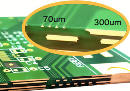
3, Via-in-Pad Technology: Via-in-pad technology allows vias to be placed directly under surface-mount components' pads, reducing signal distortion and improving thermal performance. Advanced heavy copper PCB manufacturing processes enable the efficient filling of these vias with conductive materials to enhance reliability. 4, Back Drilling: Back drilling involves removing the unused portion of vias that pass through multiple layers of a PCB. This technique is crucial for heavy copper PCBs with high layer counts to minimize signal reflections, impedance mismatch, and crosstalk issues. 5, Etching Process: Since etching is a horizontal handle process, etching chemistry is sprayed on both of top and bottom sides. While the chemistry that is sprayed from the bottom falls back off the panel, the chemistry sprayed from the top side still remains on the panel, then forming a puddle. As a result, the bottom side is often over-etched. Because of the etch rate on the top side of the panel is reduced. This requires the operator to slow down the line speed in order to properly etch the top surface. |
6, Thermal Management Solutions: Advanced heavy copper PCBs may incorporate specialized thermal management solutions, such as embedded heat sinks, metal core construction, or thermal vias, to enhance heat dissipation and improve overall performance in high-power applications. 7, Selective Plating: Selective plating allows for the targeted deposition of copper on specific areas of the PCB, such as pads, traces, or vias. This technique is utilized in heavy copper PCB manufacturing to ensure uniform copper distribution and precise copper thickness control for optimal current handling capability. 8, Advanced Surface Finishes: Heavy copper PCBs may employ advanced surface finishes, such as ENIG (Electroless Nickel Immersion Gold), OSP (Organic Solderability Preservatives), or HASL (Hot Air Solder Leveling), to enhance solderability, corrosion resistance, and overall reliability of the board. By incorporating these advanced techniques into the manufacturing process, heavy copper PCBs can meet the demanding requirements of high-power applications while maintaining superior performance, reliability, and durability. |
|
Advantages of Heavy Copper PCB : |
1, Improved Reliability: Heavy copper PCBs exhibit better reliability and longevity due to their enhanced thermal dissipation and reduced voltage drop. This results in improved overall system performance and reduced risk of component failure. 2, Higher Current Carrying Capacity: Heavy copper PCBs can handle higher current levels due to their increased copper weight. This is particularly beneficial in applications that require efficient power distribution and high-power handling capabilities. |
|
 |
3, Suitability for High-Power Applications: Heavy copper PCBs are specifically designed to meet the requirements of high-power applications, such as power supplies, automotive electronics, industrial equipment, and renewable energy systems. They offer the necessary current carrying capacity and thermal management capabilities for such demanding applications. 4, Reduced Voltage Drop: The increased copper weight in heavy copper PCBs helps to minimize voltage drops, ensuring stable and reliable power distribution throughout the board. This is especially important in high-power applications where voltage fluctuations can impact performance. 5, Enhanced Mechanical Strength: Heavy copper PCBs have greater mechanical strength and durability due to their thick copper layers. This makes them more resistant to mechanical stress, bending, and vibration, increasing the overall robustness of the PCB. |
6, Design Flexibility: Despite their increased copper weight, heavy copper PCBs can still be designed with complex layouts, fine traces, and controlled impedance. This allows for greater flexibility in designing high-power circuits without compromising performance. 7, Improved Thermal Management: The additional copper in heavy copper PCBs helps to dissipate heat more effectively. This feature is crucial in applications where thermal management is critical to maintain optimal performance and prevent overheating of components. Heavy Copper PCBs provide advantages in terms of current handling capacity, thermal management, mechanical strength, voltage stability, reliability, and design flexibility. These advantages make them well-suited for applications that require high power handling, efficient thermal dissipation, and reliable performance. |
|
Design Challenging of Heavy Copper PCB : |
1, Trace Width and Spacing: Heavy copper PCBs require wider trace widths and spacing to accommodate the higher current levels they are designed to handle. Designers must carefully calculate and optimize these parameters to ensure the necessary current carrying capacity without sacrificing board space or signal integrity. 2, Heat Dissipation: Heavy copper PCBs generate more heat due to their increased copper weight. Effective heat dissipation is crucial to prevent overheating of components and ensure reliable operation. Designers need to incorporate appropriate thermal management techniques such as thermal vias, heat sinks, or metal core construction to efficiently dissipate heat. |
|
 |
3, Board Flexibility: The additional copper weight in heavy copper PCBs reduces the board's flexibility. This can pose challenges when it comes to bending or fitting the PCB into tight spaces. Designers must carefully consider the mechanical requirements and constraints of the application to ensure the board's mechanical strength and flexibility are appropriate. 4, Manufacturability: Heavy copper PCBs require specialized manufacturing processes to achieve the desired copper weight and maintain consistent copper distribution on the layers. These processes may involve sequential lamination, controlled impedance design, and selective plating, which can add complexity and cost to the manufacturing process. 5, Cost: Heavy copper PCBs are generally more expensive to manufacture compared to standard PCBs due to the increased copper weight and specialized manufacturing processes involved. Designers need to balance the benefits of heavy copper with the cost considerations of the project. |
6, Signal Integrity: Heavy copper PCBs can introduce challenges related to signal integrity, particularly in high-speed or high-frequency applications. Careful attention must be given to controlled impedance design, proper grounding techniques, and minimizing signal reflections and crosstalk. 7, Assembly and Soldering: The increased copper weight and thickness in heavy copper PCBs can impact the assembly and soldering processes. Designers must ensure proper component placement, pad design, and solder mask considerations to facilitate successful assembly and soldering. By addressing these design challenges and working closely with our experienced engineers, designers can overcome the complexities associated with heavy copper PCBs and develop robust and reliable designs for high-power applications. |
|
Typical Applications of Heavy Copper PCB : |
Heavy copper PCBs are commonly used in various high-power and high-reliability applications that require superior current handling capacity, thermal management, and durability. Some typical applications of heavy copper PCBs include: 1, Medical Devices: Heavy copper PCBs are utilized in medical devices and equipment such as MRI machines, X-ray systems, defibrillators, and patient monitoring systems. The high current carrying capacity and thermal performance of heavy copper PCBs ensure the reliable operation of critical medical electronics. 2, Power Supplies: Heavy copper PCBs are widely used in power supply units, such as AC/DC converters, DC/DC converters, and inverters. The increased copper weight allows for efficient power distribution and high current carrying capacity, making them ideal for power electronics applications. 3, Industrial Equipment: Heavy copper PCBs are employed in industrial equipment, including motor drives, automation systems, control panels, and power distribution units. Their ability to handle high currents and dissipate heat effectively makes them suitable for industrial applications requiring reliable and efficient performance. |
|
 |
4, Automotive Electronics: Heavy copper PCBs are utilized in automotive electronics for applications such as electric vehicles (EVs), hybrid electric vehicles (HEVs), battery management systems, engine control units (ECUs), and lighting systems. They offer robust performance in high-temperature environments and demanding operating conditions. 5, Renewable Energy Systems: Heavy copper PCBs play a vital role in renewable energy systems, such as solar inverters, wind turbine controllers, and energy storage systems. These applications benefit from the enhanced current carrying capacity and thermal management capabilities of heavy copper PCBs to ensure reliable operation and maximize energy efficiency. 6, Aerospace and Defense: Heavy copper PCBs are used in aerospace and defense applications that demand high reliability, ruggedness, and performance under extreme conditions. They are employed in avionics systems, radar systems, communication equipment, and military electronics where durability and thermal management are critical. |
7, Telecommunications: Heavy copper PCBs find application in telecommunications infrastructure, including base station equipment, data centers, and networking devices. They provide the necessary power handling capabilities and thermal dissipation required for reliable data transmission and communication services. Heavy Copper PCBs are essential components in a wide range of high-power applications across industries that prioritize performance, reliability, and efficiency. Their unique characteristics make them well-suited for demanding environments where standard PCBs may not meet the requirements for power handling and thermal management. |
|
Why PANDA PCB for Power Supply PCB ? |
At PANDA PCB, we are your trusted partner for all your Power Supply PCB needs. With a reputation for excellence and innovation, here's why you should choose PANDA PCB for your heavy copper PCB projects: ● Expertise in Power Supply PCBs: Our team of experienced engineers specializes in designing and manufacturing heavy copper PCBs to meet the highest standards of quality and performance. We have the expertise to deliver customized solutions tailored to your specific requirements. |
|
 |
● Advanced Manufacturing Capabilities: Equipped with state-of-the-art facilities and advanced manufacturing technologies, PANDA PCB ensures precision and reliability in every heavy copper PCB we produce. We have a special treament for solder mask protect layer, only printed the heavy copper conductors with "Line-Mask" process firstly , then using "E-spray" process to jet the solder mask for the whole surface. also can utilizes a unique process refers to as “Laminated Deposition”, This combination of processes allows extreme copper thickness requirements to become very practical and cost effective. ● Reliability and Durability: PANDA PCB heavy copper PCBs are built to last, offering superior reliability and durability in even the most demanding applications. Trust us to provide robust solutions that meet your stringent performance criteria. ● Thermal Management Solutions: With our heavy copper PCBs, effective heat dissipation is guaranteed. We understand the importance of thermal management in high-power applications and design our PCBs to optimize and ensure consistent performance. |
● Cost-Effective Solutions: While maintaining uncompromised quality, PANDA PCB offers cost-effective solutions for heavy copper PCB projects. We strive to provide competitive pricing without compromising on the excellence of our products. Choose PANDA PCB for your Power Supply PCB requirements and experience the difference in quality, reliability, and performance. Contact us today to discuss your project needs and let us help you achieve success with our top-notch heavy copper PCB solutions. |
|
Engineering Capabilities of Heavy Copper PCB : |
|
|