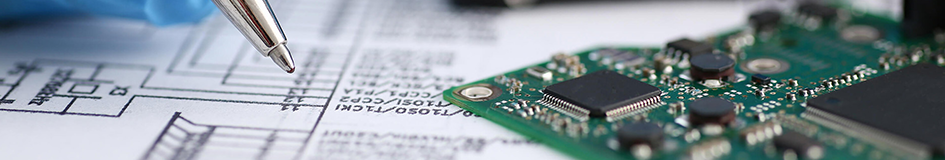
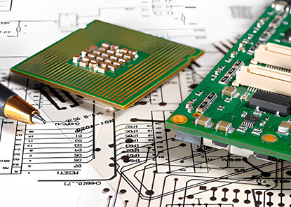
PCB Reverse Engineering Services
PCB Reverse Engineering involves analyzing and deconstructing an existing printed circuit board (PCB) to rebuild its design, functionality, and schematic, typically when the original design files are unavailable, with the goal of restoring or replicating the circuit board’s structure and functionality, and is commonly used in product development, repair, upgrades, and competitive analysis. PCB Reverse Engineering involves using reverse engineering techniques to analyze a physical circuit board and restore its original design files, bill of materials (BOM), and production files (such as Gerber files, CAD drawings, and specifications). This process begins by carefully disassembling the PCB, identifying its components, and analyzing its electrical pathways. Advanced tools, such as X-ray imaging, scanning electron microscopy (SEM), and automated optical inspection (AOI), are often used to inspect and map the circuit board’s structure in detail. PCB Reverse Engineering is widely used in various fields such as product development to recreate or improve existing designs, repairs to identify and fix faulty components, upgrades to enhance the functionality of outdated circuit boards, and competitive analysis to study and replicate successful designs when the original design files are inaccessible, enabling innovation and cost-effective solutions in electronic manufacturing. Basic Process of PCB Reverse Engineering : |
 |
|
 |
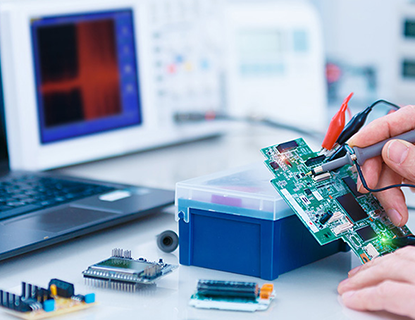
1, Image Capture and Analysis: ● X-ray Imaging: X-ray technology is used to penetrate the PCB layers and capture images of internal structures, especially for multi-layer PCBs, where X-ray imaging is a crucial tool. ● Layer Stripping: PCB is physically stripped layer by layer to obtain detailed images of each layer. This method can reconstruct the PCB's structure but damages the sample. 2, Image Processing and Editing: |
|
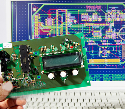
3, Layout Reconstruction: 4, Schematic Creation: 5, Bill of Materials (BOM) Creation: 6, Functional Validation: |
||
Applications of PCB Reverse Engineering : |
 |
1, Product Development: 2, Repair and Upgrades: 3, Competitive Analysis: 4, Intellectual Property Protection: |
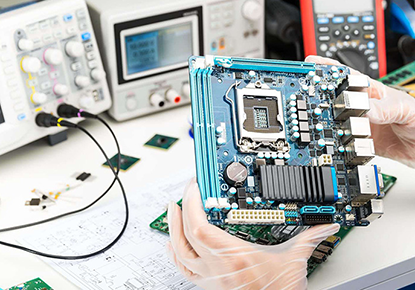
Tools and Techniques of PCB Reverse Engineering : |
1, Scanners and Microscopes: 2, Signal Analyzers: 3, EDA Software: 4, X-ray Imaging and CT Scanning: |
Why Perform PCB Reverse Engineering ? |
 |
1, Repair and Maintenance: 2, Cloning and Improvement: 3, Product Analysis and Innovation: 4, Copyright Protection and Patent Verification: |
Types of PCB Reverse Engineering Service : |
1, Destructive Reverse Engineering: 2, Non-Destructive Reverse Engineering: |
Challenges of PCB Reverse Engineering : |
 |
● Complexity: As PCB design becomes more advanced, modern boards can have up to 32 layers and high component density, increasing the difficulty of reverse engineering. ● Time and Cost: Depending on the complexity of the circuit board, reverse engineering can take anywhere from days to weeks, with costs ranging from thousands to tens of thousands of dollars. ● Accuracy Issues: Ensuring that the reverse-engineered design matches the original is critical. Any minor discrepancies could result in functional differences. PCB Reverse Engineering is a complex but valuable technique that is widely used in various sectors, including product development, repair, upgrades, and competitive analysis. As PCB technology advances and reverse engineering tools improve, this technique will become more efficient and accurate, playing a crucial role in the innovation and protection of electronic products in the future. |
Advantages of PCB Reverse Engineering : |
● Cost Reduction: Reverse engineering allows companies to replicate or improve existing designs without starting from scratch, reducing development costs. ● Rapid Innovation: Reverse engineering speeds up product iteration and market launch by quickly obtaining detailed information on existing products. ● Enhanced Competitive Advantage: By analyzing competitors' designs, companies can identify flaws or improvements, gaining an edge in the market. ● Increased Control: Reverse engineering reduces reliance on external design teams, enabling companies to independently modify designs and troubleshoot issues. Looking for reliable PCB Reverse Engineering Services? Our company specializes in providing comprehensive PCB reverse engineering solutions to help you restore lost design files, create accurate bill of materials (BOM), and generate production files like Gerber Files, CAD Drawings, and Specifications. Whether you're looking to replicate an existing PCB, improve an outdated design, or conduct competitive analysis, our expert team ensures precise, high-quality results that match the original functionality of your circuit board. Let us help you bring your product back to life with cutting-edge technology and expert analysis! Contact us today for a consultation. |