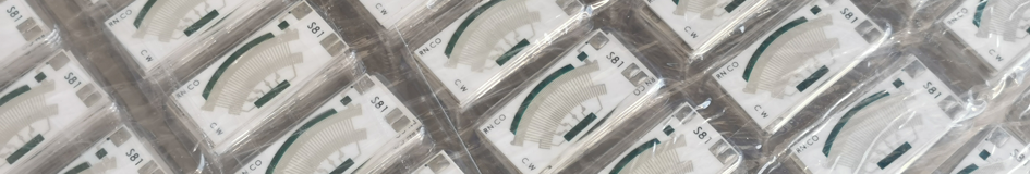
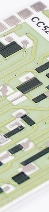
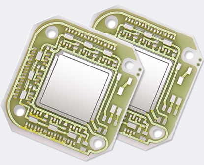
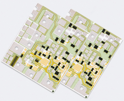
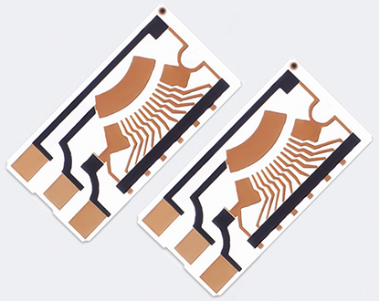
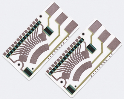
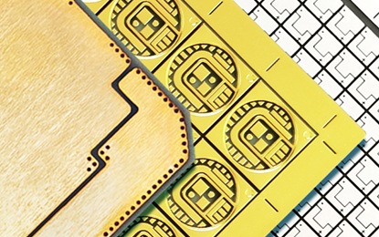
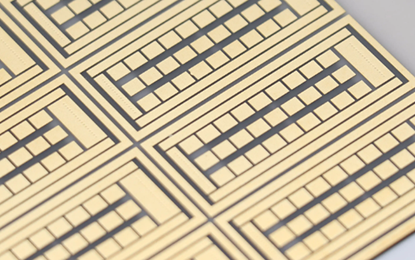
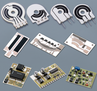
Thick Film Substrates
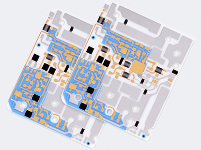
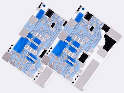
Thick Film Substrates are advanced electronic materials used for hybrid microcircuits and integrated electronics, typically made from ceramics, metals, or glass for their electrical insulation, thermal stability, and mechanical strength, with the process involving screen printing conductive patterns, resistors, capacitors, and other passive components onto the substrate followed by high-temperature firing to bond them, creating reliable, highly integrated circuits ideal for applications in automotive, aerospace, and industrial electronics where performance and durability are crucial. Thick Film Substrates are known for their versatility and durability, making them ideal for applications that require high reliability and excellent thermal performance. Their unique combination of properties, such as resistance to extreme environmental conditions, makes them essential for a wide range of electronic and microelectronic applications. Ceramic materials, such as alumina (Al2O3), aluminum nitride (AlN), and beryllium oxide (BeO), are commonly used because of their superior electrical and thermal conductivity. Thick Film Substrates also offer significant advantages in terms of integration, as they allow resistors, capacitors, and other circuit components to be directly integrated onto the substrate. This eliminates the need for discrete components, leading to more compact and efficient circuit designs. The integration reduces both the assembly complexity and manufacturing costs, while ensuring that the components maintain optimal electrical, thermal, and mechanical performance over time. Advantages of Thick Film Substrates : |
 |
|
 |
1, Higher Reliability : 2, Wider Temperature Range : 3, Higher Precision on Resistors : |
|
4, Low Coefficient of Thermal Expansion (CTE) : 5, More Compact, Efficient Package, Economical : |
||
 |
6, Low Failure Rate : 7, Small Size And Weight : 8, Excellent Thermal Insulation : 9, Custom Packaging : |
|
10, High Frequency : For more relevant technical introductions, please refer to Thick Film Technology. |
||
Process Features of Thick Film Substrates : |
1, Substrates Selection: |
|
 |
2, Screen-Printing: 3, Drying and Sintering: |
4, Multilayer Hybrid Circuits Structure: |
|
 |
5, Through-Hole Metallization: 6, Laser Trimming: |
7, Inspection Process: |
|
Why Deed to Customize Thick Film Substrates ? |
Custom Thick Film Substrates are often necessary to meet the specific requirements of various applications in the electronics industry. Here are several reasons why customization is not just an option, but a critical aspect of using these substrates: 1. Application-Specific Requirements: |
|
 |
2. Improved Thermal Management: 3. Regulatory Compliance: 4. Miniaturization: |
5. Integration of Components: 6. Regulatory Compliance: |
|
 |
7. Environmental Resistance: 8. Innovation and Competitive Edge: 9. Enhanced Electrical Properties: |
Custom Thick Film Substrates are essential for achieving the highest levels of performance, reliability, and innovation in electronic devices. It enables manufacturers to create products that are perfectly suited to their intended use, providing a competitive advantage in a rapidly evolving market. |
|
Types of Sintering Technology for Thick Film Substrates : |
Thick Film Substrates are ceramic materials commonly used in electronic packaging and circuit fabrication. There are two main types based on sintering temperature: High-Temperature Co-fired Ceramic (HTCC) and Low-Temperature Co-fired Ceramic (LTCC). These two technologies differ significantly in terms of material composition, sintering temperature, and applicable ranges, making them suitable for different electronic applications. |
|
 |
1. High-Temperature Co-fired Ceramic (HTCC) 1.2, Applications: |
1.3, Characteristics: ● Higher material strength: Due to the use of high-temperature ceramics, HTCC materials have greater structural strength, allowing them to withstand significant mechanical stress. ● Larger substrate sizes: HTCC is suitable for larger circuit substrates and provides good electrical isolation performance. ● Complex processing: Due to the high sintering temperature, the process requires precise control, making it more complex and expensive compared to other technologies. |
|
 |
2. Low-Temperature Co-fired Ceramic (LTCC) 2.2, Applications: |
2.3, Characteristics: ● High-density integration: LTCC allows for the integration of high-density circuits and multi-layer designs. Multiple circuit layers can be incorporated into a single substrate, making it ideal for miniaturized, complex electronics. ● Excellent electrical properties: LTCC provides outstanding electrical performance, especially for high-frequency applications, with good electrical insulation that helps reduce signal loss. ● Miniaturization suitability: LTCC substrates support multi-layer circuits and small-size designs, ideal for highly integrated, miniaturized devices. ● Lower mechanical strength: Compared to HTCC, LTCC has somewhat lower mechanical strength and may not be suitable for applications requiring large mechanical stress. High-Temperature Co-fired Ceramic (HTCC) is more suitable for high-temperature environments, applications requiring higher mechanical strength, and larger substrates, such as high-frequency circuits and power electronics. Low-Temperature Co-fired Ceramic (LTCC) is ideal for small-size, high-density, and multi-layer circuit designs, particularly in applications such as high-frequency communications, sensors, and micro-packaging. Both technologies have their strengths and are chosen based on specific application needs, including operating conditions, electrical performance, and design complexity. |
|
Comparison of HTCC and LTCC Usd For Thick Film Substrates : |
Characteristic: |
HTCC (High-Temperature Co-fired Ceramic) |
LTCC (Low-Temperature Co-fired Ceramic) |
Sintering Temperature: |
Higher, typically 850°C to 1200°C |
Lower, typically below 850°C |
Materials: |
Mainly high-temperature ceramics like alumina, aluminum oxide |
Mainly glass ceramics, ceramic powders |
Applicable Products: |
High-frequency electronics, microwave circuits, RF circuits, power circuits |
High-density multi-layer circuits, sensor modules, communication devices |
High-temperature Resistance: |
Excellent, suitable for high-temperature environments |
Lower, suitable for standard or low-temperature environments |
Electrical Properties: |
Good, suitable for high-power circuits |
Excellent, suitable for high-frequency circuits and miniaturized designs |
Mechanical Strength: |
High, can withstand significant mechanical stress |
Lower, suitable for low-stress environments |
Processing Complexity: |
Relatively complex, requires higher sintering temperatures |
Simpler, allows multi-layer circuit integration |
Substrate Size |
Suitable for larger substrates |
Suitable for small-sized, highly integrated circuits |
Applications of Thick Film Substrates : |
Thick Film Substrates are extensively utilized across various industries due to their exceptional properties, such as thermal stability, high reliability, and the ability to withstand harsh conditions. Here are some specific applications of thick film ceramic substrates: 1, Industrial Control Systems: Thick film substrates find applications in industrial control systems, including motor drives, power supplies, and programmable logic controllers (PLCs). |
|
 |
2, Telecommunications: In the telecommunications industry, thick film substrates are used in the production of RFID tags for wireless communication. 3, Consumer Electronics: Thick film substrates are employed in various consumer electronic devices, including smartphones, tablets, and wearables. 4, Energy Systems: Thick film substrates are used in energy systems like solar inverters, wind power converters, and battery management systems. 5, Gas Sensors: For aerospace applications, thick film substrates are used in the development of gas sensors, which are crucial for detecting volatile organic compounds and other gases in the air. 6, Power Electronics: They are also used in power electronics for their ability to handle high power and voltage requirements, making them suitable for use in various power conversion and distribution systems. |
7, Aerospace Industry: Ceramic matrix composites (CMCs), which include thick film substrates, are increasingly used in aerospace applications due to their high-temperature resistance, wear resistance, and excellent mechanical properties at high temperatures. Thick film substrates are utilized in components like turbine blades and vanes where cooling technologies, such as film cooling, are crucial for maintaining the safe operation of hot end parts of the engine. |
|
 |
8, Automotive Systems: Thick film substrates are used in automotive systems for engine control modules and other applications where high temperatures and mechanical shock are common. The substrates' ability to dissipate heat and withstand vibrations makes them ideal for these conditions. 9, Medical Sensors: In the medical field, thick film substrates are employed in the development of sensors for monitoring vital signs, including temperature, pressure, and oxygen levels. Their properties make them suitable for use in sensitive medical equipment. 10, Digitally-Driven Hybrid Manufacture: Recent advancements include the development of digitally-driven hybrid manufacturing processes that combine ceramic paste extrusion with sacrificial support printing and micro-machining to produce three-dimensional ceramic green-state parts. This approach allows for the production of precision-engineered ceramic substrates with high densities and minimal shrinkage, suitable for various electronic applications. |
Thick Film Substrates are used in the creation of multi-layer circuit boards that are essential for complex electronic devices. These substrates provide the necessary support and insulation for the conductive layers within the circuit boards. These applications highlight the versatility and importance of thick film substrates in modern technology, from enhancing the performance of aerospace engines to improving patient care through medical sensors. |
|
Main Applications of Thick Film Substrates in Automotive Electronics : |
Thick Film Substrates play a significant role in automotive electronics due to their ability to withstand harsh environmental conditions, provide thermal management, and integrate multiple components into a compact space. Some key applications of thick film substrates in the automotive industry include: 1, Engine Control Units (ECUs): Thick film substrates are used in the manufacturing of ECUs, which are essential for controlling various engine functions such as fuel injection, throttle valve sensor, Ignition module, ignition timing, and emissions control. The high-temperature stability and reliability of thick film substrates make them suitable for these critical components. |
|
 |
2, Sensors and Actuators: Thick film substrates serve as platforms for fabricating sensors and actuators used in automotive systems. These include temperature sensors, pressure sensors, oxygen sensors (O2 sensors), and various actuation devices that are integrated onto the substrate to monitor and control engine and vehicle functions. 3, Telematics and Infotainment Systems: Thick film substrates are utilized in telematics units and infotainment systems, supporting wireless communication, GPS navigation, voltage regulater, fuel level sensor, entertainment features, and connectivity functions within vehicles. 4, LED Lighting Modules: Automotive lighting systems, including LED headlights and taillights, utilize thick film substrates for mounting LED chips and associated circuitry. These substrates provide a reliable platform for driving and controlling the lighting functions in vehicles. 5, On-Board Diagnostics (OBD): Thick film substrates are integrated into on-board diagnostic systems that monitor and report the performance of various vehicle systems. These systems rely on reliable thick film substrates to ensure accurate data collection and processing. |
6, Electronic Control and Monitoring Systems: Thick film substrates are used in various electronic control and monitoring systems within vehicles, such as transmission control units, anti-lock braking systems (ABS), airbag control modules, and vehicle stability control systems. These substrates support the integration of control electronics and sensor interfaces. 7, Power Modules: Thick film substrates are employed in the production of power modules for automotive applications, including motor drive systems, voltage regulators, and power converters. The thermal conductivity and electrical performance of thick film technology are valuable for managing power electronics in vehicles. Thick Film Substrates contribute to the performance, reliability, and miniaturization of electronic systems in modern automobiles, helping to meet the demanding requirements of the automotive industry for ruggedness, temperature resistance, and long-term functionality. |
|
Design Guidelines of Thick Film Substrates : |
We compiled a Thick Film Substrates-Design Guidelines as attached for you to download, It is to better support our customers' needs in designing and applying Thick Film Substrates, This guide covers detailed information on product solutions, engineering design specifications, material properties, available manufacturing processes, and more. We hope that this guide will assist customers in standardizing their design process while ensuring the manufacturability of the design data, ultimately improving product reliability and production efficiency. Customers are encouraged to refer to the guide when designing Thick Film Substrates to ensure adherence to best practices. |
Capabilities of Thick Film Substrates Are As Follows : |
1, Optional Processes of Thick Film Substrates :
Metalization Types : |
Thick Film Substrates (Screen-Printed) |
Thin Film Substrates (Photo-Imaged) |
|||
Process Types : |
TFM Capabilities |
HTCC / LTCC Capabilities |
DBC Capabilities |
DPC Capabilities |
AMB Capabilities |
Layer Counts : |
1, 2, 3, 4, 5, 6 Layers |
1, 2, 4, 6, 8, 10, 12 Layers |
1, 2 Layers |
1, 2 Layers |
1, 2 Layers |
Max Board Dimension : |
200*230mm |
200*200mm |
138*178mm |
138*190mm |
114*114mm |
Min Board Thickness : |
0.25mm |
0.25mm |
0.30mm~0.40mm |
0.25mm |
0.25mm |
Max Board Thickness : |
2.2mm |
2.0mm |
1L: 1.6mm; 2L 2.0mm |
2.0mm |
1.8mm |
Conductor Thickness : |
10um - 20um |
5um - 1500um |
1oz - 9oz |
1um - 1000um |
1oz- 22oz |
Min Line Width/Space : |
8/8mil (0.20/0.20mm) |
6/6mil (0.15/0.15mm) |
10/10mil (0.25/0.25mm) |
6/6mil (0.15/0.15mm) |
12/12mil (0.30/0.30mm) |
Substrates Types : |
AI203, ALN, BeO, ZrO2 |
AI203, ALN, BeO, ZrO2 |
Al2O3, AlN, ZrO2, PbO, SiO2, ZTA, Si3N4, SiC, Sapphire, Polycrystalline Silicon, Piezoelectric Ceramics |
Al2O3, AlN, ZrO2, PbO, SiO2, ZTA, Si3N4, SiC, Sapphire, Polycrystalline Silicon, Piezoelectric Ceramics |
AI203, ALN, BeO, ZrO2, Si3N4 |
Min Hole Diameter : |
4mil (0.15mm) |
4mil (0.15mm) |
4mil (0.1mm) |
4mil (0.1mm) |
4mil (0.1mm) |
Outline Tolerance : |
Laser: +/-0.05mm; Die Punch: +/-0.10mm |
Laser: +/-0.05mm; Die Punch: +/-0.10mm |
Laser: +/-0.05mm; Die Punch: +/-0.10mm |
Laser: +/-0.05mm; Die Punch: +/-0.10mm |
Laser: +/-0.05mm; Die Punch: +/-0.10mm |
Substrate Thickness : |
0.25, 0.38, 0.50, 0.635, 0.80,1.0, 1.25, 1.5, 2.0mm, Customizable |
0.25, 0.38, 0.50, 0.635, 0.80,1.0, 1.25, 1.5, 2.0mm, Customizable |
0.25, 0.38, 0.50, 0.635, 0.80,1.0, 1.25, 1.5, 2.0mm, Customizable |
0.25, 0.38, 0.50, 0.635, 0.80,1.0, 1.25, 1.5, 2.0mm, Customizable |
0.25, 0.38, 0.50, 0.635, 0.80,1.0, 1.25, 1.5, 2.0mm, Customizable |
Thickness Tolerance : |
0.25-0.38: +/-0.03mm; 0.50-2.00: +/-0.05mm |
0.25-0.38: +/-0.03mm; 0.50-2.00: +/-0.05mm |
0.25-0.38: +/-0.03mm; 0.50-2.00: +/-0.05mm |
0.25-0.38: +/-0.03mm; 0.50-2.00: +/-0.05mm |
0.25-0.38: +/-0.03mm; 0.50-2.00: +/-0.05mm |
Surface Treatment : |
Ag, Au, AgPd, AuPd |
Ag, Au, AgPd, AuPd, Mn/Ni |
OSP/Ni Plating, ENIG |
OSP/ENIG/ENEPIG |
OSP/ENIG/ENEPIG |
Min Solder PAD Dia : |
10mil (0.25mm) |
10mil (0.25mm) |
8mil (0.20mm) |
6mil (0.15mm) |
8mil (0.20mm) |
2, Engineering Specification of Thick Film Substrates :
Items : |
Typical Values |
Advanced Capabilities |
1, Substrates : |
FR4, Ceramic ( AI203, ALN, BeO, ZrO2), Polyimide (Flexible PI), Stainless Steel (SUS304), Mica |
FR4, Ceramic ( AI203, ALN, BeO, ZrO2), Polyimide (Flexible PI), Stainless Steel (SUS304), Mica |
2, Conductor (Paste) Materials : |
Copper, Silver , Gold , Silver-Palladium, Palladium-Gold, Platinum-Silver, Platinum-Gold |
Copper, Silver , Gold , Silver-Palladium, Palladium-Gold, Platinum-Silver, Platinum-Gold |
3, Thick Film Carbon Thickness (Height) : |
15um +/-5 um |
30um +/-5 um |
4, Conductor Thickness (Height) : |
12um+/-5um |
20um+/-5um |
5, Min Width of Thick Film Line : |
0.30 mm +/-0.05 mm |
0.20 mm +/-0.05 mm |
6, Min Space of Thick Film Line : |
0.30 mm +/-0.05 mm |
0.20 mm +/-0.05 mm |
7, Min Overlap (Carbon to Conductor) : |
No less than 0.25mm |
0.20mm (Minimum) |
8, Sheet Resistivity (ohms/square): |
Printed resistors in milli ohm to mega ohm range (Customizable) with tolerances of 1-10% are fabricated and protected with overglaze materials. |
Printed resistors in milli ohm to mega ohm range (Customizable) with tolerances of 0.5-10% are fabricated and protected with overglaze materials. |
9, Resistor Value Tolerance (ohms) : |
+/-10.0% (Standard) (Customizable) |
+/-0.5% (Laser trimming) |
10, Linearity : |
+/-1.0% (Standard) (Customizable) |
+/-0.2 ~ +/-0.5% (Laser trimming) |
11, Synchronism of Double Channels : |
+/-2.0% (Standard) (Customizable) (Potentiometers) |
+/-1.0% (Laser trimming) (Potentiometers) |
12, Durability of Carbon Ink (Life time) : |
0.5 Million (Min), 2.0 Million (Standard) |
5.0-10.0 Million (Max) with Surface Polishing |
13, Working Temperature : |
- 40ºC /+150ºC |
- 40ºC /+180ºC |
3, Optional Materials of Thick Film Substrates :
Substrates : |
Alumina (Al2O3) |
Aluminum Nitride (AlN) |
Beryllium Oxide (BeO) |
Zirconium Dioxide (ZrO2) |
Max Application Temperature : |
662 - 1832 |
1832 |
2300 |
2432 |
Max Power Density (W/in²): |
75 |
1010 |
250 |
300 |
Max Ramp Up Speed (°F/sec): |
122 |
572 |
400 |
350 |
Thermal Conductivity (W/mK): |
20-35 |
180-220 |
200-300 |
2.0-5.0 |
Density (g/cm³): |
3.75 |
3.26 |
2.8 |
5.9 |
Dielectric Loss: |
0.0001 - 0.001 |
0.0001 - 0.0005 |
0.0001 - 0.0002 |
0.0005 - 0.001 |
Dielectric Constant: |
9.4 - 10.2 |
8.5 - 9.0 |
6.0 - 7.0 |
25 - 30 |
CTE, ppm/ºC: |
6.0 - 8.0 |
4.0 - 5.0 |
7.0 - 9.0 |
10.0 - 11.0 |
Substrate Thickness (mm): |
0.25 - 2.0 |
0.25 - 2.0 |
0.25 - 2.0 |
0.25 - 2.0 |
Typical Max. Dimension (inch): |
6 x 12 |
5 x 11 |
6 x 6 |
4 x 4 |
Theoretical Total Wattage (W): |
5400 |
55000 |
15000 |
20000 |
4, Conductive Paste of Thick Film Substrates :
Paste ( Materials) : |
Conductor Width/Space |
Soldering / Bonding |
Gold : |
8/8mil (0.20/0.20mm) |
Gold is a good conductor material and allows thermo-compression gold wire bonding and eutectic die attachment. It is, of course, costly and has poor solderability. |
Silver : |
8/8mil (0.20/0.20mm) |
Soldering & Silver is lower in cost, and solderable, but is not leach-resistant with tin/lead solders.More seriously, silver atoms migrate under the influence of DC electric fields, both causing short-circuits and reacting with many of the resistor paste formulations. |
Platinum-Silver : |
6/6mil (0.15/0.15mm) |
Soldering & Surface Mount, Palladium and platinum alloyed to the gold and silver produce good conductor pastes,with good adhesion to the substrate, good solderability, and moderately good wire bonding characteristics. Copper and nickel are examples of materials that have been proposed for paste systems as substitutes for noble metals. |
Palladium-Silver : |
8/8mil (0.20/0.20mm) |
Soldering & Surface Mount ,Solderable, Wire bondable, (good aged adhesion general purpose), Silver-palladium conductor inks are the most commonly used materials, with both price and performance (primarily resistance to solder) increasing with palladium content. |
Platinum-Gold : |
6/6mil (0.15/0.15mm) |
Soldering & Au or Al Wire Bonding, Solderable (excellent aged adhesion with no migration). |
Palladium-Gold : |
8/8mil (0.20/0.20mm) |
Soldering & Au or Al Wire Bonding, Wire bondable. |
5, Resistive Paste of Thick Film Substrates :
Performances : |
Common Values/Range |
Description |
Resistance Value : |
1Ω to several MΩ |
The resistance value depends on the type and ratio of carbon black, typically ranging from 1Ω to Mega ohm. |
Resistance Tolerance : |
±1% to ±10% |
High-precision resistors can achieve ±0.1% tolerance used laser trimming process. |
Temperature Coefficient (TCR) : |
±50ppm/°C to ±200ppm/°C |
High-quality resistive paste should have a low TCR, preferably below ±100ppm/°C. |
Stability : |
≤1% |
Resistors must undergo high-temperature aging and humidity tests to ensure stability. |
Sintering Temperature : |
850°C to 950°C |
The sintering temperature for carbon paste depends on material properties, typically in this range. |
Conductivity : |
10⁶ S/m to 10⁸ S/m |
Conductivity depends on the type and ratio of carbon black, affecting resistance precision and stability. |
Surface Smoothness : |
Ra≤ 1 μm |
The surface must be free of cracks, bubbles, and non-uniform layers to ensure good mechanical and electrical properties. |
Insulation Resistance : |
≥10⁹ Ω |
Carbon paste should have good insulation properties to avoid leakage or short circuits. |
Mechanical Strength : |
≥100 MPa |
The resistive layer must have good compressive and bending strength to ensure the reliability of the resistor. |
Volatility : |
Solvent residue ≤ 1% |
High volatility solvents help with even coating and drying, but excessive volatility may affect electrical performance. |
Oxidation Resistance : |
>1000 hours |
High-quality carbon paste should have strong oxidation resistance to extend the service life. |
Humidity Resistance : |
≥1000 hours |
Resistors should be able to withstand high-humidity conditions to ensure long-term stable performance, no significant changes. |
6, Dielectric Paste of Thick Film Substrates :
The dielectric paste used in Thick Film Substrates is a crucial component that provides insulation and protection for the underlying circuitry. The specifications for dielectric paste in thick film substrates may include: 1, Dielectric Constant (ε): This parameter measures the ability of the material to store electrical energy when exposed to an electric field. It's an important factor in determining the capacitance and impedance of the substrate. 2, Dielectric Strength: Also known as breakdown voltage, this specification indicates the maximum electric field that the dielectric paste can withstand without experiencing electrical breakdown. 3, Insulation Resistance: This specification measures the resistance of the dielectric material to electrical current flow, which is essential for maintaining the integrity of the circuitry and preventing leakage currents. 4, Thermal Conductivity: The ability of the dielectric paste to conduct heat away from the circuitry, helping to dissipate heat and maintain the reliability of the components. 5, Thermal Coefficient of Expansion (TCE): TCE specifies how the dimensions of the dielectric material change with temperature variations. Matching the TCE of the dielectric paste to that of the substrate material helps prevent mechanical stress and cracking during thermal cycling. 6, Firing Temperature: Similar to the resistive paste, the firing temperature of the dielectric paste is important to achieve proper adhesion and performance without damaging the substrate or other components. 7, Composition: The composition of the dielectric paste, including the type and amount of ceramic fillers, glass frits, and other additives, influences its electrical, thermal, and mechanical properties. |
7, Insulating Paste of Thick Film Substrates :
Commonly used non-metallic materials for protective coatings include overglazes (glass glaze), enamel, polymers, and epoxies, depending on the application conditions and environment. The insulating-protective layer for a custom heating element or ceramic resistor is typically printed or continuously coated to cover the heater assembly as the sheath of the heating element or ceramic resistor. This serves several purposes: 1, Mechanical protection: It helps to safeguard the heating element from physical damage. 2, Electrical insulation: The coating insulates the heating traces, preventing electrical leakage or short circuits. 3, Corrosion prevention and water resistance: It acts as a barrier against corrosion and protects the heating element from moisture damage. 4, Thermal resistance: The coating should be able to withstand the maximum application temperatures without degrading or melting. 5, Vacuum protection: In high vacuum environments, the coating prevents outgassing and maintains the integrity of the heating element. 6, High voltage resistance: It enables the heating element to withstand high voltage without breakdown or electrical failure. |