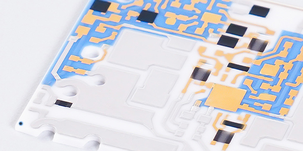
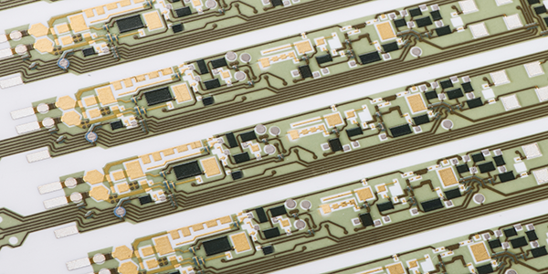
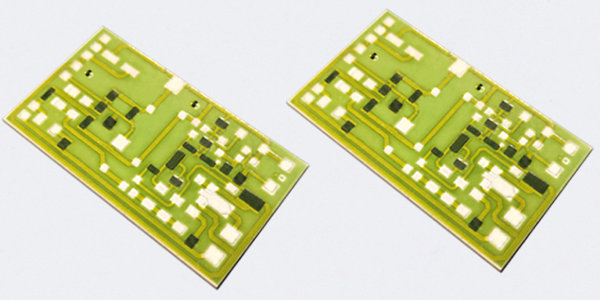
Multilayer Thick Film Substrates
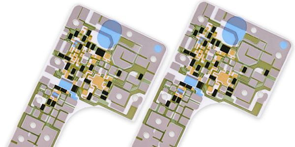
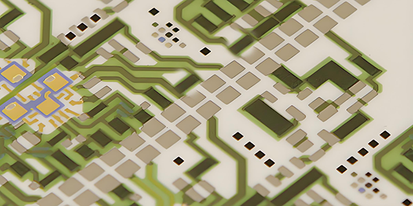
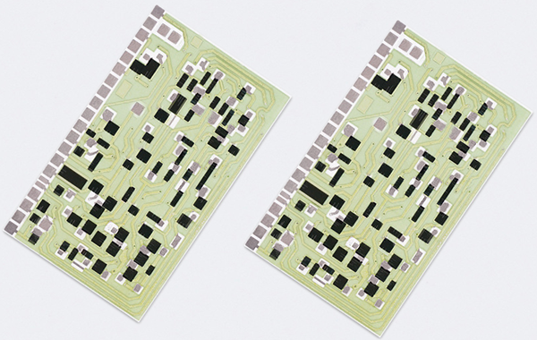
Multilayer Thick Film Substrates, also called Thick Film Multilayer Substrates, are created using thick film technology with ceramic as the base material, consisting of multiple conductive layers (such as gold, silver, silver-palladium) with functional circuit patterns printed layer by layer through sintering, where each layer has specific properties like conductivity, insulation, or shielding, and is sintered at high temperatures using materials like metal oxides, metal powders, and glass matrices, which enhances circuit density and integration while ensuring stable, reliable electrical performance.
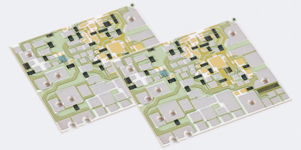
Multilayer Thick Film Substrates offer high-density integration, superior mechanical strength, and excellent thermal stability. By employing a multilayer structure (such as 2-layer or 4-layer circuits), these substrates can realize more complex circuit designs, support higher levels of functional integration, and are suitable for devices with limited space. The thick film materials can withstand high temperatures and currents, ensuring stable performance in harsh environments. Additionally, the electrical properties of these substrates include low resistance, low noise, and strong anti-interference capability, making them advantageous in high-precision applications. The products also feature good thermal conductivity, effectively dissipating heat and reducing the risk of circuit failure due to overheating.
Thick Film Multilayer Substrates are widely used in various electronic products and devices, particularly in fields that require high integration and high performance. For instance, they are commonly used in automotive electronics, communication equipment, medical instruments, industrial automation, and consumer electronics. In automotive electronics, these substrates are used in components like sensors and control modules, where they can operate reliably in extreme temperatures and vibration conditions. In the communication sector, they are employed in RF modules and high-frequency circuits to ensure signal transmission quality. In medical equipment, due to their reliability and durability, Multilayer Thick Film Substrates are used to manufacture critical electronic components.
Features of Multilayer Thick Film Substrates :
Multilayer Thick Film Substrates are fabricated using thick film technology, involving multiple layers of conductive materials (such as gold or silver pastes) and dielectric insulating layers, which are sequentially screen-printed and sintered to build a ceramic substrate with multiple integrated circuitry layers. This process allows for the creation of substrates with higher circuit densities compared to conventional single- or double-layer ceramic substrates. Here are the key features of Multilayer Thick Film Substrates:
● High Circuit Density:
By using a multilayer design (e.g., 3-layer, 4-layer, 5-layer, or 6-layer configurations), these substrates achieve significantly higher circuit density than traditional single- or double-layer ceramics. This enables the integration of more complex and compact circuits within a smaller area, making them ideal for miniaturized electronic devices.
● Multilayer Structure:
The use of multiple layers (conductive and dielectric) allows for more sophisticated circuit designs, including interlayer vias for electrical connections between layers. This multilayer approach enables the realization of complex functions and high-performance electronic circuits that require both high density and small size.
● Improved Electrical and Thermal Performance:
Multilayer Thick Film Substrates provide excellent electrical properties such as low resistance and minimal signal noise, ensuring high-quality electrical performance. The layers also exhibit good thermal conductivity, helping to dissipate heat efficiently and maintain stable operating conditions even under high current or temperature stress.
● Design Flexibility:
The thick film technology enables flexible design options for both conductive and insulating layers. Different layers can be customized for specific electrical properties (e.g., high conductivity in signal paths, insulating properties in non-conductive areas), allowing for complex, multi-functional circuit designs within a single substrate.
● Durability and Reliability:
The sintering process used to create the substrate results in high mechanical strength, ensuring the substrate can withstand harsh operating environments. These substrates also offer excellent resistance to thermal cycling, vibration, and mechanical stress, making them reliable in demanding applications such as automotive, industrial, and medical electronics.
● Customizable Functional Layers:
The substrates feature conductive layers (often silver, gold, or silver-palladium) for signal routing and dielectric layers for insulation, which can be tailored to suit the specific requirements of the circuit design. This enables engineers to create specialized solutions for high-frequency, high-power, or signal-sensitive applications.
● Compact and Space-Saving:
By stacking multiple conductive and insulating layers, the overall substrate remains compact and space-efficient. This is particularly advantageous for applications where size constraints are critical, such as in sensors, medical devices, and high-performance communication systems.
● High Temperature and High Current Handling:
Multilayer Thick Film Substrates are designed to withstand high operating temperatures and currents without degradation of performance. This feature is essential for applications in automotive electronics, industrial control systems, and other environments with extreme conditions.
● Cost-Effective Manufacturing:
While the multilayer design is more complex than single-layer substrates, the use of thick film technology with screen printing offers a cost-effective production process. The ability to manufacture multiple layers simultaneously and the use of relatively low sintering temperatures reduce overall manufacturing costs.
● Electromagnetic Interference (EMI) Shielding:
The multilayer structure can effectively shield against electromagnetic interference, improving the overall signal integrity of high-frequency circuits and ensuring stable performance in environments with significant external electrical noise.
Multilayer Thick Film Substrates combine high-density circuit integration with enhanced electrical and thermal performance, providing a durable, compact, and reliable solution for complex electronic applications. Their ability to integrate multiple functional layers and withstand extreme conditions makes them a preferred choice for advanced industries such as automotive electronics, telecommunications, medical devices, and industrial automation.
Challenges of Multilayer Thick Film Substrates :
Multilayer Thick Film Substrates offer many advantages, but there are several challenges and limitations associated with their design, manufacturing, and application that can impact performance, cost, and reliability, with some of the key challenges outlined below:
1. Manufacturing Complexity and Cost :
● Multilayer Build Process: The process of creating multilayer thick film substrates involves several stages of screen printing, drying, sintering, and bonding layers. Each additional layer increases the complexity of the process. Accurate alignment of layers and vias, as well as controlling the thickness of the printed films, requires high precision.
● Manufacturing Cost: The increased complexity of the multilayer process often results in higher production costs compared to simpler single-layer or double-layer substrates. The materials, additional processing steps, and precision required can increase the overall cost of the finished substrate.
2. Layer Alignment and Registration :
● Alignment Challenges: One of the most critical issues in the fabrication of multilayer thick film substrates is maintaining proper alignment between the layers. Misalignment between layers can lead to short circuits, poor electrical contact, or signal integrity problems.
● Via Interconnections: Proper alignment of vias (vertical interconnections between layers) is essential for ensuring the correct electrical connections. Any misalignment can result in faulty connections, requiring rework or scrapping of the substrate.
3. Via Integrity and Electrical Performance :
● Via Quality: Creating vias that are conductive and reliable is a major challenge. Improper via formation can result in high resistance, poor signal transmission, or even complete failure of interlayer connections. Achieving high-quality via construction with thick film materials is more difficult than in thin-film substrates.
● Signal Integrity: Multilayer thick film substrates can suffer from signal integrity issues, particularly in high-frequency applications. Impedance matching, crosstalk between layers, and interference between the conductive layers need to be carefully managed to avoid performance degradation.
4. Material Selection and Compatibility :
● Material Compatibility: The materials used for the conductive and insulating layers must have compatible thermal expansion coefficients to prevent stress and potential delamination during thermal cycling. Incompatibilities between materials can result in cracks, delamination, or failure under mechanical stress.
● Material Cost and Availability: Specialized materials (e.g., high-performance conductive pastes, high-quality dielectric materials) can be costly and may not always be readily available. The choice of materials also impacts the performance of the substrate in terms of thermal, electrical, and mechanical properties.
5. Thermal Management :
● Heat Dissipation: As the number of layers increases, managing the heat generated during operation becomes more challenging. In high-power applications, the thermal resistance between layers can increase, making heat dissipation less efficient. Proper thermal design is critical to prevent overheating and ensure reliable operation.
● Thermal Stress: Multilayer substrates experience thermal stress during heating and cooling cycles. If the thermal expansion of the materials is not properly matched, it can lead to warping, cracks, or layer delamination, affecting the overall reliability of the device.
6. Limited Frequency Range for High-Speed Circuits :
● High-Frequency Limitations: Multilayer thick film substrates may face limitations in high-frequency applications (e.g., RF, microwave, and high-speed digital circuits) due to parasitic inductance, capacitance, and signal loss between the layers. The conductive traces, vias, and dielectric materials used in thick-film technology may not be ideal for high-frequency signal transmission.
7. Durability and Reliability Under Harsh Conditions :
● Mechanical Stress and Impact: While multilayer thick film substrates are generally robust, they can still be vulnerable to mechanical stress, especially in applications involving vibration or shocks. The adhesive bonds between layers and the thickness of the materials used can make the substrate susceptible to cracking or delamination under extreme mechanical loads.
● Environmental Degradation: Over time, exposure to harsh environmental conditions (e.g., moisture, chemical exposure, UV radiation) can degrade the performance of multilayer thick film substrates. The protective coatings and materials used may not be sufficient to prevent long-term degradation in certain environments.
8. Limited Flexibility :
● Rigid Nature: Multilayer thick film substrates are typically rigid, making them unsuitable for flexible or wearable applications. The materials and fabrication techniques used in thick film technology do not lend themselves well to producing flexible circuits.
● Customization Complexity: While multilayer substrates can be designed with customized layers for specific functions, making significant changes or modifications to the design after production has started can be difficult and costly.
9. Size and Integration Limitations :
● Size Constraints: Although multilayer thick film substrates can achieve high circuit density, they are still limited by the overall size of the ceramic substrate. For highly miniaturized or integrated systems (such as in advanced semiconductor packaging), other technologies (e.g., thin-film, organic, or microelectronic packaging) might offer better solutions.
● Integration with Other Components: Integrating multilayer thick film substrates with other components such as integrated circuits (ICs), passive components, or microelectromechanical systems (MEMS) may be more challenging compared to other types of substrates. The differences in material properties and fabrication methods can result in issues related to bonding, assembly, and testing.
While Multilayer Thick Film Substrates offer significant advantages in terms of high-density circuit integration, electrical and thermal performance, and reliability, they also come with challenges in terms of manufacturing complexity, material compatibility, signal integrity, and environmental concerns. Overcoming these challenges requires careful design, selection of materials, and advanced manufacturing techniques to ensure that the benefits of multilayer thick film substrates outweigh their limitations in specific applications.
Optimization Design of Thick Film Multilayer Substrates :
Thick Film Multilayer Substrates design optimization is a complex engineering task involving multiple factors such as materials, structure, electrical performance, and thermal management, and as electronic devices continue to evolve and integrate more functions, the performance requirements for these substrates have become more stringent, making design optimization crucial for ensuring reliability, stability, and cost-effectiveness, with several key aspects to consider in the process:
1. Electrical Performance Optimization :
Electrical performance is the core of Thick Film Multilayer Substrates design, especially in high-frequency and high-speed applications. Optimizing electrical performance involves the following aspects:
1.1 Signal Integrity :
To ensure signal integrity, designers need to:
● Optimize Signal Paths: The design of signal paths should minimize signal loss and delay. By using appropriate trace widths and layer interconnections (such as microstrip lines or stripline designs), signal reflection and interference can be reduced effectively.
● Impedance Control: Impedance matching is key to ensuring signal transmission quality. Different layers need to be carefully designed to match impedance, preventing signal reflection and attenuation.
Minimize Crosstalk: Crosstalk between signal and power lines can degrade signal quality. Adjusting trace spacing or adding isolation layers can help reduce crosstalk.
1.2 High-Frequency Performance :
In high-frequency applications, the substrate material and design directly affect signal propagation speed and loss:
● Low Loss Materials: Choosing materials with low dielectric constants and loss factors can reduce signal loss at high frequencies. Common low-loss materials include certain ceramics and polymer-based substrates.
● Precise Layer Thickness Control: Controlling the inter-layer thickness is crucial, as it influences the speed of electromagnetic wave propagation and signal attenuation.
1.3 Electromagnetic Compatibility :
Electromagnetic interference (EMI) and electromagnetic compatibility are critical in high-frequency, densely integrated designs. To optimize EMC:
● Power and Ground Layer Configuration: A well-designed power and ground layer configuration can help reduce EMI. Typically, power and ground layers are placed as internal layers, with shielding designs that minimize noise interference.
● Shielding Design: Adding shielding layers in critical areas helps reduce electromagnetic radiation from other parts of the circuit, ensuring stable operation in complex electromagnetic environments.
2. Thermal Management Design :
As the power of electronic devices increases, effective thermal management becomes increasingly important, especially in high-power and multi-layer systems. The design should consider how to efficiently dissipate heat to prevent overheating and performance degradation.
2.1 Thermal Conductive Materials Selection :
Choosing materials with good thermal conductivity is essential to address thermal management:
● Thermal Conductive Ceramic Materials: Ceramic materials are often used due to their excellent thermal conductivity, which helps transfer heat from heat sources to the exterior of the substrate, preventing localized overheating.
● Thermal Conductive Copper and Metal Substrates: In some applications, metal-based substrates (such as copper or aluminum) can enhance thermal conductivity and heat dissipation.
2.2 Heat Dissipation Layer Design :
Including heat dissipation layers in the substrate design can help dissipate heat more effectively. Common methods include:
● Thermal Distribution Layers: A well-designed thermal distribution layer helps spread heat evenly, preventing hot spots.
● Heat Sinks or Channels: Adding heat sinks or creating heat channels helps dissipate heat, particularly in high-power, dense designs.
2.3 Thermal Expansion Matching :
Materials expand at different rates when heated, so thermal expansion matching between layers is important in Thick Film Multilayer Substrates design. Ensuring thermal expansion compatibility can prevent cracking or failure of connections due to mismatched expansion rates.
3. Layer Structure and Multilayer Integration :
One of the defining features of Thick Film Multilayer Substrates is their multi-layered structure. The design of each layer must account for electrical functionality and mechanical stability.
3.1 Interlayer Connections :
In multilayer substrates, interconnections between circuits are vital. Optimizing these connections can enhance both electrical performance and mechanical strength:
● Vertical Interconnection Technology: Using vias for interlayer connections ensures tighter and more stable electrical contacts.
● Precise Via Design: Via size, location, and shape must be carefully designed to ensure good electrical connection while minimizing signal interference and reflection.
3.2 Increased Integration :
As technology advances, there is a greater demand for higher integration in electronic devices. Designers can increase integration through:
● Functional Integration: Combining more functions into a single substrate reduces the number of external components, thereby reducing size, cost, and system complexity.
● Multifunctional Integrated Layers: By integrating power management, signal processing, and thermal functions in the same substrate, designers can reduce the number of layers and connections, improving overall performance and reliability.
4. Material Selection and Optimization :
Materials play a key role in the performance of Thick Film Multilayer Substrates. The choice of materials directly affects electrical performance, thermal performance, and mechanical strength.
4.1 Ceramic Material Selection :
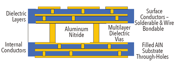
Ceramic substrates are widely used in multilayer thick film designs due to their excellent electrical and thermal properties. Common ceramic materials include Al2O3 (alumina) and AlN (aluminum nitride). These materials offer high temperature resistance, corrosion resistance, and excellent electrical properties.
4.2 Conductor Material Selection :
Conductive layers are usually made from precious metals (such as gold or silver) or alloys to ensure good conductivity and stable electrical contact. With technological advancements, new conductive materials, such as nano-conductive materials, are being incorporated into designs to enhance electrical performance and stability.
5. Manufacturing Processes and Quality Control :
Design optimization must also take into account practical manufacturing processes and quality control:
● Manufacturing Tolerance Control: In Thick Film Multilayer Substrates, the alignment, spacing, and connections between layers must be strictly controlled. Even the smallest error can affect electrical performance and mechanical reliability.
● Surface Treatment and Coating Processes: Surface treatments (such as gold plating or silver coating) significantly affect corrosion resistance, conductivity, and solderability. Optimizing surface treatment processes is essential for improving overall quality.
Thick Film Multilayer Substrates design optimization is a complex, multidisciplinary process that involves electrical, thermal, and structural considerations. As electronic devices become smaller, more integrated, and more powerful, optimizing the design of these substrates becomes increasingly important. By selecting appropriate materials, optimizing interlayer connections, controlling thermal management, and improving electrical performance, designers can ensure that Thick Film Multilayer Substrates deliver excellent performance and reliability in high-frequency, high-power, and highly integrated applications.
For more information, Please refer to Thick Film Substrates.

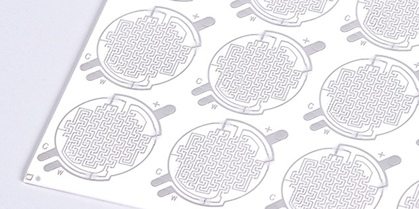
Custom Thick Film Sensors
- Custom Thick Film Sensor Elements
- Fuel Level Sensor PCB
- Fuel Level Sensor Ceramic PCB
- Oil Level Sensor Ceramic PCB
- Motorcycle Fuel Level Sensor PCB
- Throttle Position Sensor PCB
- Throttle Position Sensor FR4 PCB
- Throttle Position Sensor Ceramic PCB
- Throttle Position Sensor Flexible PCB
- Accelerator Pedal Sensor PCB
- Accelerator Pedal Position Sensor PCB
- Pedal Position Sensor Carbon PCB
- Potentiometer PCB
- Linear Potentiometer Carbon Track PCB
- Rotary Potentiometer Carbon Track PCB
- FR4 Potentiometer Carbon PCB
- Ceramic Potentiometer Carbon PCB
- Flexible Potentiometer Carbon PCB
- Logarithmic Taper Potentiometer PCB
- Position Sensor PCB
- FR4 Position Sensor Carbon PCB
- Ceramic Position Sensor Carbon PCB
- Flexible Position Sensor Carbon PCB
- Flexible Sensor PCB
- Printed Flexible Electronic PCB
- Printed Carbon PCB
- Ceramic Pressure Sensors
- Ceramic Thick Film Pressure Sensors
- Engine Oil Pressure Sensor PCB
- Gold Coated Ceramic Substrates
- Gold Coated Thick Film Substrates
- Metallized Ceramic Substrates
- Multilayer Thick Film Substrates
- Thick Film Metallization Technology
- Thin Film Metallization Technology
- Thin Film Ceramic PCB
- Variable Resistor Carbon PCB
- Remote Ready Sender Ceramic PCB
- LP Gas Tank Gauges Ceramic PCB
- Thick Film Capacitive Sensors
- Thick Film Capacitive Pressure Sensors
- Thick Film Edible Oil Quality Sensors
- Thick Film Meteorological Rainfall Sensors
- PI Interdigital Electrodes (Flexible)
- Air Door Actuator PCB
- HVAC Blend Door Actuator PCB