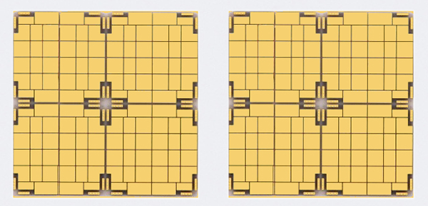
Thin Film Ceramic PCB
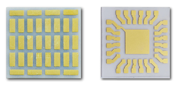
Thin Film Ceramic PCBs are high-performance printed circuit boards that combine ceramic substrates with thin film technologies to create circuits with excellent thermal conductivity, electrical performance, and high-temperature resistance, using materials like alumina, aluminum nitride, or silicon nitride, and by depositing metal or conductive layers onto the ceramic surface, thin-film circuits are formed, enabling precise electronic connections and ensuring high reliability for applications requiring advanced thermal management and electrical performance.
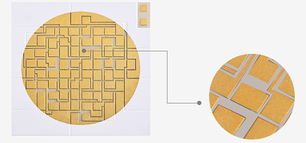
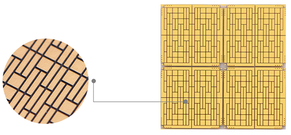
Thin Film Ceramic PCBs are manufactured using advanced techniques such as Physical Vapor Deposition (PVD), Chemical Vapor Deposition (CVD), and laser etching, which allow for precise deposition of metal films and the formation of circuits. These processes provide precise control over the thickness and layout of conductive layers on the ceramic surfaces, enabling the creation of complex circuits. Due to the superior thermal conductivity of the ceramic substrates, Thin Film Ceramic PCBs are commonly used in applications involving high-power devices and high-speed signal transmission, efficiently dissipating heat and ensuring stable system operation over time.
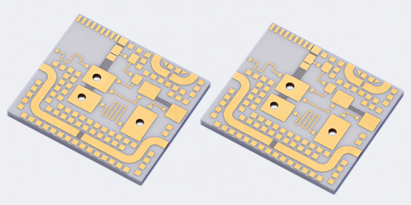
Thin Film Ceramic PCBs are ideal for high-frequency, high-power, and high-precision electronic applications due to their outstanding thermal management capabilities and support for high-density integrated circuits. These PCBs are commonly used in RF (radio frequency) modules, radar systems, laser systems, and advanced communication equipment, where high-frequency performance is critical. Additionally, their exceptional thermal conductivity and mechanical strength make them well-suited for use in automotive electronics, aerospace, and medical devices, ensuring long-term performance and stability in demanding environments.
What is Thin Film Metallization Technology ?
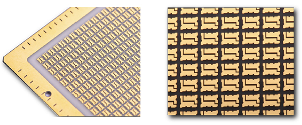
Thin Film Ceramic PCBs use Thin Film Metallization Technologies, processes in which thin layers of metal or conductive materials are deposited onto the surfaces of ceramic substrates through physical or chemical methods. These technologies allow for the creation of highly refined conductive traces on the ceramic substrates, offering high precision, excellent adhesion, and superior electrical performance. The thin-film deposition processes enable Thin Film Ceramic PCBs to meet the demands of high-frequency, high-power, and high-precision applications, making them among the most crucial technologies in the manufacture of electronic components and circuit boards.
Thin Film Metallization Technologies used in Thin Film Ceramic PCBs include several different processes, with the most common ones being Direct Plated Copper (DPC), Direct Bonded Copper (DBC), as well as DCB and AMB technologies. Direct Plated Copper (DPC) involves electroplating copper layers directly onto ceramic substrates to form conductive traces, making it suitable for high-power and high-heat load applications. Direct Bonded Copper (DBC) bonds copper layers directly to ceramic substrates, providing superior thermal conductivity, making them ideal for power modules, LED lighting, and automotive electronics. Additionally, DCB (Direct Copper Bonding) and AMB (Active Metal Brazing) technologies use specialized metal bonding processes to tightly integrate metal layers with ceramics, offering higher structural stability and thermal conductivity, and are commonly used in high-power electronic devices.
Thin Film Metallization Technologies in Thin Film Ceramic PCBs not only improve the performance of the circuits but also significantly enhance their reliability and thermal management capabilities. By utilizing these advanced deposition techniques, Thin Film Ceramic PCBs can support higher frequencies, higher power, and higher temperature working environments, making them widely used in industries such as radio frequency (RF) systems, power electronics, automotive electronics, and aerospace. The precise control of these technologies enables the circuit boards to withstand more complex electrical and thermal loads, providing longer service lives and lower failure rates.
Main Features of Thin Film Ceramic PCB :
● High Thermal Conductivity: Ceramic substrates offer better heat dissipation compared to traditional FR-4 substrates, which enhances the performance and reliability of the circuit.
● Low Dielectric Constant (Dk): Ceramic materials generally have a lower dielectric constant, which is beneficial for high-frequency applications as it reduces signal loss and improves signal integrity.
● Low Coefficient Thermal Expansion (CTE): The CTE of ceramic substrates is lower than that of FR-4, making them more resistant to temperature changes and better suited for high-temperature environments.
● Enhanced Electrical Isolation: Due to the material properties of ceramics, thin film ceramic PCBs provide superior electrical isolation, which is crucial for high-speed signal transmission.
● Chemical and Mechanical Stability: Ceramic substrates are highly resistant to chemicals and mechanical stress, making them ideal for harsh environments and long-term reliability.
● Miniaturization: The thin film process allows for the creation of very fine lines and spaces, enabling the design of compact and miniaturized electronic devices.
● Embedded Passive Components: Thin film technology enables the integration of passive components such as resistors, capacitors, and inductors directly into the substrate, reducing the overall footprint of the electronic assembly.
● Hybrid Thick-Film and Thin-Film Technologies: The combination of both thick-film and thin-film deposition techniques offers flexibility and performance optimization for high-frequency applications.
● Advanced Metallization Techniques: Thin Film Ceramic PCBs utilize advanced metallization processes, such as physical vapor deposition (PVD), to ensure a uniform and high-quality copper layer on the ceramic substrate.
● Customization and Flexibility: Thin Film Ceramic PCBs can be customized to meet specific application requirements, including multilayer designs and the integration of various passive components.
These features highlight the versatility and performance advantages of thin film ceramic PCBs, which continue to be an area of focus for innovation and development in the electronics industry.
Applications of Thin Film Ceramic PCB :
● High-Performance Electronics: Ceramic substrates are widely used in integrated circuits (ICs) for their thermal stability and electrical insulation, ensuring the longevity and performance of electronic devices under harsh conditions.
● Micro-Electro-Mechanical Systems (MEMS): The robustness and thermal stability of ceramic substrates make them ideal for MEMS devices like accelerometers, gyroscopes, and pressure sensors, which demand precision and reliability.
● LED Lighting Systems: With excellent thermal conductivity and mechanical stability, ceramic substrates are crucial in high-power LED applications, facilitating efficient heat dissipation for prolonged LED lifespan and enhanced performance.
● Power Electronic Modules: Thin Film Ceramic PCBs handle high power densities and thermal cycling effectively, providing reliable performance in power electronic modules for applications such as electric vehicles and renewable energy systems.
● Medical Equipment: The biocompatibility and stability of ceramic substrates make them suitable for medical devices, including implantable devices, wearable sensors, and diagnostic equipment, where long-term reliability and sensitivity are critical.
● Automotive Components: High-temperature resistance and mechanical strength of ceramic PCBs make them ideal for automotive electronics, such as engine control units and sensor systems, which endure extreme temperatures and vibrations.
● High-Frequency Devices: Due to their excellent electrical insulation and thermal properties, Thin Film Ceramic PCBs are preferred in high-frequency applications, including communication devices and radar systems, where signal integrity and heat management are paramount.
● Optical Coatings: Ceramic substrates are used for optical thin film coatings in applications like anti-reflection coatings, interference filters, and mirrors, enhancing optical performance in various photonic devices.
FR4 PCB VS Thin Film Ceramic PCB :
Thin Film Ceramic PCBs and traditional FR-4 material PCBs exhibit significant differences in terms of cost and performance:
● Cost: Thin Film Ceramic PCBs are generally more expensive than FR-4 PCBs due to the higher cost of ceramic materials and the more complex manufacturing process. Specialized manufacturing techniques such as laser cutting, thick-film or thin-film deposition, and co-firing processes contribute to increased production costs.
● Thermal Performance: Ceramic substrates have a much higher thermal conductivity than FR-4, making them ideal for high-power applications where efficient heat dissipation is critical. The superior thermal management capability of ceramic substrates helps maintain the performance and reliability of electronic devices by preventing overheating.
● Electrical Performance: Thin Film Ceramic PCBs typically have a lower dielectric constant (Dk) than FR-4, which is beneficial for high-frequency applications as it reduces signal loss and improves signal integrity. In contrast, FR-4 has a higher dielectric constant, which may lead to more signal attenuation in high-frequency applications.
● Mechanical Properties: FR-4 material is known for its good mechanical strength and flexibility, making it suitable for applications where the PCB may undergo bending or flexing. Ceramic substrates, on the other hand, are rigid and brittle, offering excellent dimensional stability but potentially more prone to cracking or breaking under mechanical stress.
● Manufacturing Complexity: The processing difficulty for ceramic PCBs is higher than for FR-4 PCBs. The brittle nature of ceramics requires careful handling during production to avoid damage. Additionally, specialized manufacturing techniques may be needed, which can increase the complexity and cost of production.
● Application Scope: Due to their performance characteristics, Thin Film Ceramic PCBs are often used in applications that demand high thermal management and electrical performance, such as aerospace, medical devices, automotive, and high-performance computing. FR-4, due to its cost-effectiveness and adequate performance, is suitable for a broad range of applications, including consumer electronics, telecommunications, and industrial equipment.
Thin Film Ceramic PCBs may be more costly, they offer significant advantages in thermal management, electrical performance, and mechanical stability, particularly for applications requiring high performance and reliability. FR-4 provides a balanced choice between cost and performance, making it suitable for a wide array of electronic applications.
For more information, Please refer to Ceramic PCB.
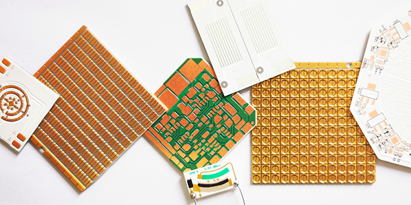
Custom Thick Film Sensors
- Custom Thick Film Sensor Elements
- Fuel Level Sensor PCB
- Fuel Level Sensor Ceramic PCB
- Oil Level Sensor Ceramic PCB
- Motorcycle Fuel Level Sensor PCB
- Throttle Position Sensor PCB
- Throttle Position Sensor FR4 PCB
- Throttle Position Sensor Ceramic PCB
- Throttle Position Sensor Flexible PCB
- Accelerator Pedal Sensor PCB
- Accelerator Pedal Position Sensor PCB
- Pedal Position Sensor Carbon PCB
- Potentiometer PCB
- Linear Potentiometer Carbon Track PCB
- Rotary Potentiometer Carbon Track PCB
- FR4 Potentiometer Carbon PCB
- Ceramic Potentiometer Carbon PCB
- Flexible Potentiometer Carbon PCB
- Logarithmic Taper Potentiometer PCB
- Position Sensor PCB
- FR4 Position Sensor Carbon PCB
- Ceramic Position Sensor Carbon PCB
- Flexible Position Sensor Carbon PCB
- Flexible Sensor PCB
- Printed Flexible Electronic PCB
- Printed Carbon PCB
- Ceramic Pressure Sensors
- Ceramic Thick Film Pressure Sensors
- Engine Oil Pressure Sensor PCB
- Gold Coated Ceramic Substrates
- Gold Coated Thick Film Substrates
- Metallized Ceramic Substrates
- Multilayer Thick Film Substrates
- Thick Film Metallization Technology
- Thin Film Metallization Technology
- Thin Film Ceramic PCB
- Variable Resistor Carbon PCB
- Remote Ready Sender Ceramic PCB
- LP Gas Tank Gauges Ceramic PCB
- Thick Film Capacitive Sensors
- Thick Film Capacitive Pressure Sensors
- Thick Film Edible Oil Quality Sensors
- Thick Film Meteorological Rainfall Sensors
- PI Interdigital Electrodes (Flexible)
- Air Door Actuator PCB
- HVAC Blend Door Actuator PCB