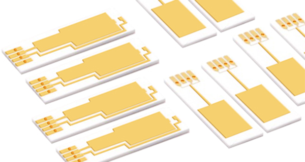
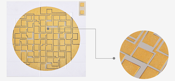
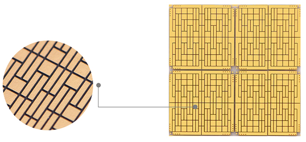
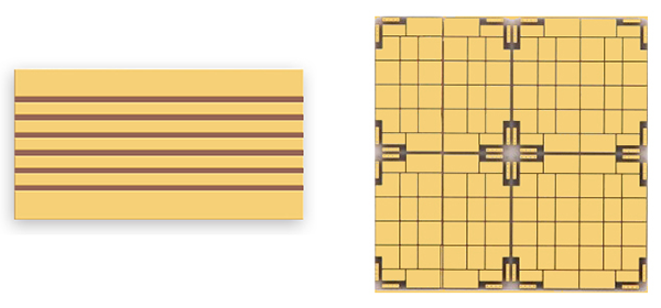
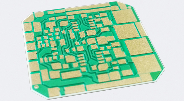
Thin Film Metallization Technology
Thin Film Metallization Technologies, also called Thin Film Ceramic Metallization Technologies, integrate thin metal layers onto ceramic materials, enabling the combination of ceramics with electronic components through methods like sputtering, a physical vapor deposition (PVD) technique, as well as Active Metal Brazing (AMB), Direct Copper Plating (DPC), Direct Bond Copper (DBC), and cold spraying, which apply metals, alloys, oxides, or nitrides onto ceramic surfaces with high precision and excellent adhesion, such as the DBC method, which forms strong bonds by oxidizing copper on ceramic surfaces and using a eutectic liquid phase.
Thin Film Metallization Technologies enhance the thermal, electrical, and mechanical properties of ceramic substrates. The metal layers, typically made from copper or other conductive materials, improve the circuits’ electrical performance while ensuring high thermal conductivity and heat dissipation. These technologies enable the production of circuits that can withstand high-power loads, making them suitable for demanding applications. Moreover, the integration of ceramics with metals improves the structural stability of the components, which is essential in environments requiring high reliability and thermal management. These qualities make Thin Film Ceramic PCBs highly reliable and effective in various electronic systems.
Thin Film Ceramic Metallization Technologies are widely used in industries requiring high-frequency, high-power, and high-precision components. These include radio frequency (RF) systems, power electronics, automotive electronics, aerospace, and LED lighting. The superior thermal conductivity and mechanical strength provided by the metal-ceramic bonds make Thin Film Ceramic PCBs ideal for power modules, radar systems, medical devices, and automotive applications where temperature stability and performance are critical. Additionally, these technologies support high-density integrated circuits, contributing to the advancement of modern electronic devices that demand both high efficiency and reliability in extreme conditions.
Advantages of Thin Film Metallization Technology :
● High Precision and Fine Detail:
Thin Film Metallization Technology allows for the creation of precise, finely detailed conductive traces on ceramic substrates. This is particularly beneficial for applications that require highly accurate and small-scale circuits, ensuring consistent performance in high-frequency and high-power environments.
● Improved Thermal and Electrical Performance:
The metal layer applied through Thin Film Metallization improves the thermal conductivity and electrical performance of the ceramic substrates. This enhancement ensures that the components can effectively dissipate heat, reduce electrical resistance, and manage power efficiently, making it ideal for high-performance applications like power modules and RF systems.
● Strong Mechanical Bonding:
Methods like Direct Bond Copper (DBC) and Active Metal Brazing (AMB) create strong, durable bonds between metals and ceramics. These bonds increase the structural stability of the components, ensuring long-lasting reliability even under harsh conditions, such as high temperatures and mechanical stress.
● Versatility Across Materials:
Thin Film Metallization Technology can be used with a wide range of materials, including metals, alloys, oxides, and nitrides. This versatility allows manufacturers to tailor the metallization process to suit specific application requirements, whether for high-frequency circuits, power electronics, or other specialized needs.
● Cost-Effectiveness for High-Volume Production:
The ability to apply metal layers uniformly and with high precision makes Thin Film Metallization an efficient process, especially when scaling up for mass production. It reduces material waste and allows for cost-effective manufacturing, which is essential for industries that rely on high-volume production.
● Enhanced Reliability and Durability:
By improving both the thermal and electrical properties of ceramic substrates and providing robust mechanical bonds, Thin Film Metallization ensures higher reliability and durability of the components. This is particularly important for mission-critical applications in sectors like aerospace, automotive, and medical devices, where failure is not an option.
Applications of Thin Film Metallization Technology :
Thin Film Metallization Technologies are renowned for their exceptional performance in high-tech applications due to their superior thermal and electrical properties. Here are some representative applications of thin film ceramic PCBs:
● High-Performance Electronics: Ceramic substrates are widely used in integrated circuits (ICs) for their thermal stability and electrical insulation, ensuring the longevity and performance of electronic devices, even under harsh conditions.
● Micro-Electro-Mechanical Systems (MEMS): The robustness and thermal stability of ceramic substrates make them ideal for MEMS devices such as accelerometers, gyroscopes, and pressure sensors, which require precision and reliability.
● LED Lighting Systems: Known for their excellent thermal conductivity and mechanical stability, ceramic substrates are crucial in high-power LED applications, where efficient heat dissipation is necessary for prolonged LED lifespan and enhanced performance.
● Power Electronic Modules: Ceramic PCBs are used in power electronic modules for their ability to handle high power densities and thermal cycling, providing reliable performance in applications such as electric vehicles and renewable energy systems.
● Medical Equipment: The biocompatibility and stability of ceramic substrates make them suitable for various medical devices, including implantable devices, wearable sensors, and diagnostic equipment, where long-term reliability and sensitivity are critical.
● Automotive Components: The high-temperature resistance and mechanical strength of ceramic PCBs make them ideal for use in automotive electronics, such as engine control units and sensor systems, which are subjected to extreme temperatures and vibrations.
● High-Frequency Devices: Due to their excellent electrical insulation and thermal properties, ceramic PCBs are preferred in high-frequency applications, such as communication devices and radar systems, where signal integrity and heat management are paramount.
● Optical Coatings: Ceramic substrates are utilized for optical thin film coatings in applications like anti-reflection coatings, interference filters, and mirrors, enhancing optical performance in various photonic devices.
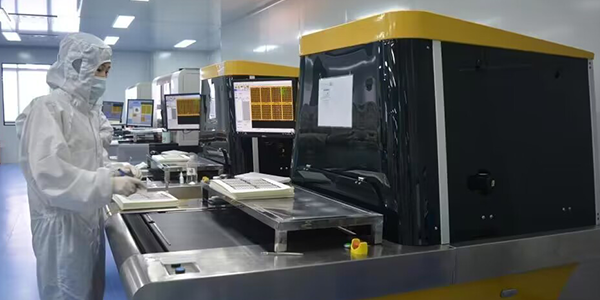
Processes of Thin Film Ceramic Metallization Technology :
Thin Film Ceramic Metallization Technologies are critical processes in the manufacturing of high-performance electronic devices, particularly for power electronics packaging and advanced ceramic substrates. These processes involve several key steps and techniques that ensure the quality, reliability, and performance of the final products.
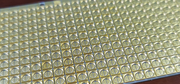
● Substrate Preparation: This involves the selection and preparation of the ceramic substrate, which could be materials like alumina (Al2O3), silicon nitride (Si3N4), or aluminum nitride (AlN). The substrate may undergo surface treatment to ensure proper adhesion of the metal layer.
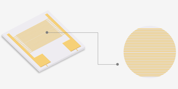
● Deposition of Thin Film: Thin films of metals are deposited onto the ceramic substrate using techniques such as Physical Vapor Deposition, Chemical Vapor Deposition, or sputtering. These methods allow for precise control of the thickness and uniformity of the metal layer.
● Adhesion Layer: To enhance the bonding between the ceramic and the metal layer, an adhesion layer (such as titanium or titanium-tungsten) is often used. This layer improves the interfacial strength and prevents delamination.
● Conductive Layer: Following the adhesion layer, a conductive layer, typically made of metals like gold, silver, or platinum, is deposited. This layer forms the electrically active part of the metallization and may involve patterning to create specific circuitry designs.
● Barrier Layer: In some cases, a barrier layer is used to protect the underlying layers from diffusion or other interactions with subsequent layers in the metallization stack. This could include metals like platinum, palladium, or nickel.
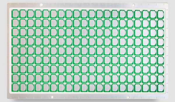
● Patterning: The metallization layers are then patterned to create the desired circuitry using techniques such as photolithography, etching, or laser ablation. This step is crucial for defining the functional structures on the ceramic substrate.
● Characterization and Testing: After the metallization process, the ceramic substrate undergoes various tests to evaluate the quality of the metal layers, including surface morphology, resistivity, and interfacial strength. Techniques such as atomic force microscopy, dual electrometry four-probe method, and nano-scratch test method may be used.
● Post-Processing: This may include annealing the metallized substrate to improve the adhesion and conductivity of the metal layers, as well as any necessary cleaning or surface finishing processes.
● Integration with Other Components: The metallized ceramic substrate is then integrated with other components to complete the electronic device, which may involve processes such as wire bonding, flip-chip bonding, or the use of solder for attaching components.
These processes must be carefully controlled and optimized to ensure the high performance and reliability required for applications in power electronics, aerospace, medical devices, and other high-tech fields.
For more information, Please refer to Thin Film Substrates.
Custom Thick Film Sensors
- Custom Thick Film Sensor Elements
- Fuel Level Sensor PCB
- Fuel Level Sensor Ceramic PCB
- Oil Level Sensor Ceramic PCB
- Motorcycle Fuel Level Sensor PCB
- Throttle Position Sensor PCB
- Throttle Position Sensor FR4 PCB
- Throttle Position Sensor Ceramic PCB
- Throttle Position Sensor Flexible PCB
- Accelerator Pedal Sensor PCB
- Accelerator Pedal Position Sensor PCB
- Pedal Position Sensor Carbon PCB
- Potentiometer PCB
- Linear Potentiometer Carbon Track PCB
- Rotary Potentiometer Carbon Track PCB
- FR4 Potentiometer Carbon PCB
- Ceramic Potentiometer Carbon PCB
- Flexible Potentiometer Carbon PCB
- Logarithmic Taper Potentiometer PCB
- Position Sensor PCB
- FR4 Position Sensor Carbon PCB
- Ceramic Position Sensor Carbon PCB
- Flexible Position Sensor Carbon PCB
- Flexible Sensor PCB
- Printed Flexible Electronic PCB
- Printed Carbon PCB
- Ceramic Pressure Sensors
- Ceramic Thick Film Pressure Sensors
- Engine Oil Pressure Sensor PCB
- Gold Coated Ceramic Substrates
- Gold Coated Thick Film Substrates
- Metallized Ceramic Substrates
- Multilayer Thick Film Substrates
- Thick Film Metallization Technology
- Thin Film Metallization Technology
- Thin Film Ceramic PCB
- Variable Resistor Carbon PCB
- Remote Ready Sender Ceramic PCB
- LP Gas Tank Gauges Ceramic PCB
- Thick Film Capacitive Sensors
- Thick Film Capacitive Pressure Sensors
- Thick Film Edible Oil Quality Sensors
- Thick Film Meteorological Rainfall Sensors
- PI Interdigital Electrodes (Flexible)
- Air Door Actuator PCB
- HVAC Blend Door Actuator PCB