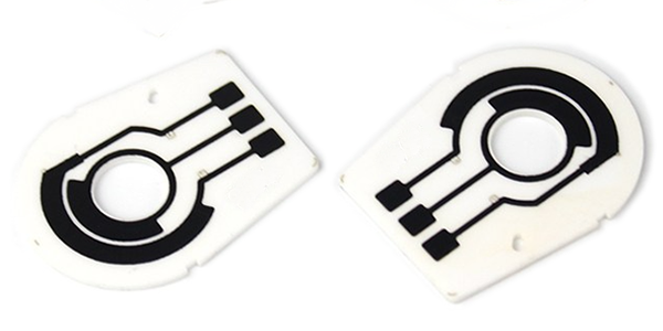
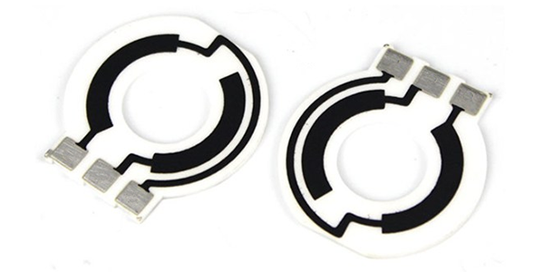
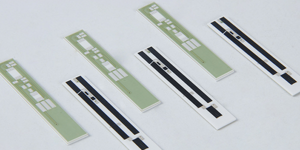
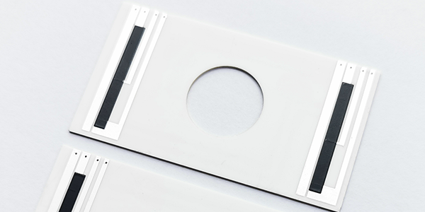
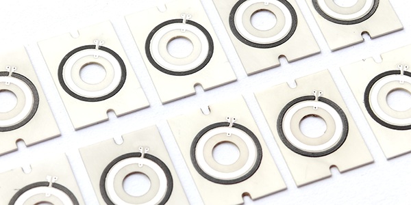
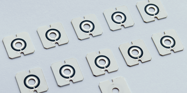
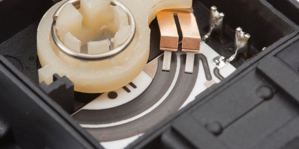
Ceramic Position Sensor Carbon PCB
Ceramic Position Sensor Carbon PCBs, also called Ceramic Position Sensor PCBs, are types of sensor circuit boards manufactured using ceramic substrates and thick-film resistor technology, widely used in the field of position sensors for efficiently and accurately detecting the linear or rotational positions of objects, with the ceramic substrates offering excellent insulation and high-temperature resistance to ensure stable performance under various environmental conditions.
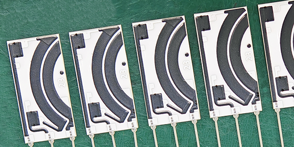
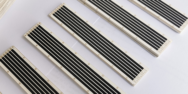
Ceramic Position Sensor Carbon PCBs feature excellent temperature resistance, reliable long-term stability, and high immunity to interference. Based on functionality, the products can be categorized into two main types: Ceramic Linear Position Sensor PCBs and Ceramic Rotary Position Sensor PCBs. Linear position sensors are typically used for detecting linear movements, while rotary position sensors focus on monitoring the angles of rotating devices. This classification allows users to choose the appropriate sensors according to specific application scenarios, enhancing the overall performance and reliability of the systems.
Ceramic Position Sensor Carbon PCBs are manufactured through a process that involves preparing the ceramic substrates, applying thick-film resistors, and printing circuits. High-purity ceramic materials are typically used to create the substrates, which are then sintered at high temperatures to form robust bases. Subsequently, thick-film resistors are applied to the surfaces of the ceramic substrates through screen printing or spraying techniques, forming circuits with specific resistance values. Finally, through precise processing and testing, each PCB is ensured to meet stringent performance standards.
Ceramic Position Sensor PCBs feature high sensitivity and stability, effectively detecting linear and rotational displacements. The linear position sensor PCBs provide real-time monitoring of linear motion, while the rotary position sensor PCBs are suitable for measuring rotational angles. These sensors not only deliver accurate position feedback but also maintain stable operation in extreme temperature and humidity conditions, making them suitable for a variety of applications, including industrial automation, automotive electronics, and medical devices.
Features of Ceramic Position Sensor Carbon PCB :
● High Thermal Conductivity: Ceramic PCBs offer higher thermal conductivity compared to FR4 PCBs, which is crucial for applications requiring efficient heat dissipation.
● Low Coefficient of Thermal Expansion: The ceramic material has a very low coefficient of thermal expansion, allowing ceramic PCBs to maintain better dimensional stability under temperature variations.
● High-Temperature Resistance: Ceramic PCBs are particularly suitable for high-temperature applications, such as those found in automotive engines, sensors, and shock absorbers.
● Excellent Electrical Insulation Strength: Ceramic PCBs exhibit high electrical insulation strength, eliminating the need for additional insulating layers and outperforming metal-based PCBs.
● No Contamination: Ceramic PCBs are free from heavy metal pollutants, such as lead (Pb), mercury (Hg), and chromium (Cr), complying with environmental regulations.
● High Mechanical Strength: At elevated temperatures, materials like silicon nitride demonstrate good mechanical strength and fracture toughness, making them suitable for vehicle modules in vibrating environments.
● Customizable Conductor Thickness: Ceramic PCBs allow for customizable conductor thicknesses to meet specific design requirements.
● High-Density Assembly: Ceramic Position Sensor Carbon PCBs support high-density assembly, making them ideal for applications with limited space.
● Low High-Frequency Loss: Ceramic PCBs exhibit low loss in high-frequency applications, making them suitable for high-frequency circuits.
● No Oxide Layer Formation: Ceramic PCBs do not form oxide layers, which helps maintain long-term stability and performance of the circuits.
● Low Organic Impurities: The low organic impurities in ceramic PCBs contribute to maintaining high efficiency, sensitivity, and accuracy of signals in high-temperature, high-vibration, and corrosive environments.
● Low Electrical Resistance: The low electrical resistance of ceramic PCBs facilitates rapid signal transmission.
Ceramic Position Sensor Carbon PCB features excellent temperature resistance, high sensitivity, and stability. It offers reliable long-term performance and is highly immune to electrical interference. The use of ceramic substrates ensures good insulation and durability, making it suitable for harsh environments. Additionally, Ceramic Position Sensor Carbon PCBs can be categorized into linear and rotary sensors, catering to diverse applications in industries such as automotive, automation, and medical devices.
Manufacturing of Ceramic Position Sensor Carbon PCB :
● Design: The process begins with circuit design and layout using specialized software, determining component placements and routing paths. This phase is crucial for the performance of the final product.
● Print Design: The PCB design is printed onto the substrate, using a plotter to create films that detail the layer specifications.
● Substrate Preparation: Suitable ceramic substrate materials are selected, covered with a uniform layer of copper foil. For multilayer boards, inter-layer connections are achieved through drilling and copper plating.
● Drilling: High-speed diamond-tipped drills or high-energy laser beams are used to create holes in the ceramic substrate, precisely etching small-diameter vias.
● Conductive Layer Printing: A conductive metal layer is printed onto the ceramic substrate and into the holes to form the desired circuit pattern. This can be accomplished through thick-film screen printing, thin-film sputtering, electroless plating, or electroplating.
● Patterning: After metallization, the conductive layer needs to be patterned to create the desired circuit layout. This is typically done using photolithography and etching processes, involving the application of a photoresist layer, exposure through a mask, developing, etching, and removal of the remaining photoresist.
● Lamination and Bonding: In multilayer ceramic PCBs, individual ceramic layers are stacked and bonded together to form a complete circuit board. This process includes aligning layers, applying bonding materials, and laminating under high pressure and temperature.
● Carbon Resistor Sintering: Carbon paste is pre-cured at high temperatures and then sintered to form resistors.
● Laser Trimming: Laser technology is used to fine-tune the resistance values to achieve linearity.
● Surface Treatment: Protective and conductive surface treatments, such as gold or nickel plating, are applied to exposed metal areas to prevent oxidation and improve solderability.
● Electrical Testing: Ceramic Position Sensor Carbon PCB undergoes electrical testing for parameters such as continuity and insulation resistance to ensure functionality and reliability.
● Visual Inspection: A visual inspection is conducted to check for any defects, such as cracks, voids, or misalignments.
These steps collectively ensure the high performance and quality of ceramic position sensor carbon PCBs, making them suitable for high-temperature, high-frequency, and high-power application environments.
Applications of Ceramic Position Sensor PCB :
Ceramic Position Sensor PCBs based on thick film resistor technology have a wide range of applications, particularly in environments that require high temperatures, high frequencies, and high power. Below are some key application areas:
● Automotive Industry: In automotive electronic systems, ceramic position sensors are used to detect vehicle speed, direction, and position. These sensors can operate reliably in high-temperature and harsh environments, enhancing vehicle safety and performance.
● Industrial Automation: In industrial robots and automation equipment, ceramic position sensors provide precise position feedback and control, ensuring efficient operation of robotic arms and other machinery.
● Aerospace: Ceramic position sensors play a crucial role in aerospace applications, capable of withstanding extreme temperatures and vibrations, providing reliable sensing information for navigation and control systems in aircraft.
● Medical Devices: In medical instruments, ceramic position sensors can be used to monitor and control the position of devices, ensuring precise operation of surgical instruments and other critical equipment.
● Consumer Electronics: In high-end consumer electronic products, such as smartphones and tablets, ceramic position sensors can enhance touch screens and other input devices, improving user experience and responsiveness.
● Energy Management: In renewable energy systems, such as wind and solar power generation, ceramic position sensors are used to monitor and adjust the position of generation equipment, optimizing energy capture efficiency.
● Military and Defense: Ceramic position sensors are used in missile guidance systems and other military equipment, ensuring high-precision operation under extreme conditions.
Due to their excellent performance and reliability, Ceramic Position Sensor PCBs based on thick film resistor technology play a key role in the aforementioned applications, driving technological advancements across various industries.
Specification of Ceramic Position Sensor PCB :
Items |
Typical Values |
1, Substrates : |
FR4, Alumina (Ceramic), Polyimide (Flexible PCB), Stainless Steel (SUS304), Mica |
2, Conductors Material : |
Copper, Silver , Gold , Silver-Palladium, Palladium-Gold |
3, Thick Film Carbon Thickness (height) : |
15um +/-5 um |
4, Silver Palladium Thickness (height) : |
12um+/-5um |
5, Minimum Width of Thick Film Traces : |
0.25 mm +/-0.05 mm |
6, Minimum Spacing of Thick Film Traces : |
0.25 mm +/-0.05 mm |
7, Minimum Footprint (Carbon to Copper) : |
No less than 0.20mm |
8, Sheet Resistivity (ohms/square): |
Printed resistors in milli ohm to mega ohm range (Customizable) with tolerances of 1-10% are fabricated and protected with overglaze materials |
9, Resistor Value Tolerance : |
+/-10.0% (Standard) (Customizable) |
10, Linearity : |
+/-1.0% (Standard) (Customizable) |
11, Synchronism of Potentiometers (Double Channels) : |
+/-2.0% (Standard) (Customizable) |
12, Durability of Carbon Ink (Life time) : |
0.5 Million (Min), 2.0-5.0 Million (Standard) |
13, Working Temperature : |
- 40℃ /+150℃ |
For more information, Please refer to Thick Film Potentiometer PCB.
Custom Thick Film Sensors
- Custom Thick Film Sensor Elements
- Fuel Level Sensor PCB
- Fuel Level Sensor Ceramic PCB
- Oil Level Sensor Ceramic PCB
- Motorcycle Fuel Level Sensor PCB
- Throttle Position Sensor PCB
- Throttle Position Sensor FR4 PCB
- Throttle Position Sensor Ceramic PCB
- Throttle Position Sensor Flexible PCB
- Accelerator Pedal Sensor PCB
- Accelerator Pedal Position Sensor PCB
- Pedal Position Sensor Carbon PCB
- Potentiometer PCB
- Linear Potentiometer Carbon Track PCB
- Rotary Potentiometer Carbon Track PCB
- FR4 Potentiometer Carbon PCB
- Ceramic Potentiometer Carbon PCB
- Flexible Potentiometer Carbon PCB
- Logarithmic Taper Potentiometer PCB
- Position Sensor PCB
- FR4 Position Sensor Carbon PCB
- Ceramic Position Sensor Carbon PCB
- Flexible Position Sensor Carbon PCB
- Flexible Sensor PCB
- Printed Flexible Electronic PCB
- Printed Carbon PCB
- Ceramic Pressure Sensors
- Ceramic Thick Film Pressure Sensors
- Engine Oil Pressure Sensor PCB
- Gold Coated Ceramic Substrates
- Gold Coated Thick Film Substrates
- Metallized Ceramic Substrates
- Multilayer Thick Film Substrates
- Thick Film Metallization Technology
- Thin Film Metallization Technology
- Thin Film Ceramic PCB
- Variable Resistor Carbon PCB
- Remote Ready Sender Ceramic PCB
- LP Gas Tank Gauges Ceramic PCB
- Thick Film Capacitive Sensors
- Thick Film Capacitive Pressure Sensors
- Thick Film Edible Oil Quality Sensors
- Thick Film Meteorological Rainfall Sensors
- PI Interdigital Electrodes (Flexible)
- Air Door Actuator PCB
- HVAC Blend Door Actuator PCB