SMT Stencil Services
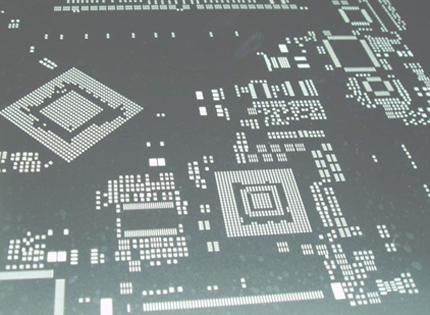
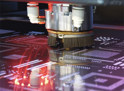
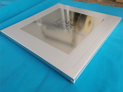
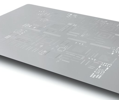
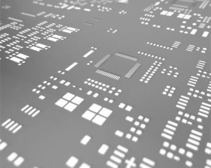
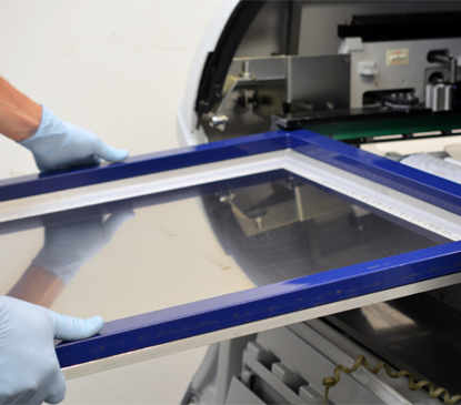
SMT Stencils, also known as Solder Paste Stencils, are precision-crafted, ultra-thin templates made from durable materials such as stainless steel or other metals, and play a pivotal role in the surface-mount technology (SMT) assembly process by enabling the accurate application of solder paste or adhesives onto printed circuit boards (PCBs), ensuring uniform deposition and precise alignment of the paste for the proper placement and reliable connection of electronic components, thereby contributing to the overall quality, integrity, and performance of the assembled circuits. SMT Stencils are typically manufactured using laser cutting or etching processes. They are placed over the PCB, and solder paste is applied through the stencil's holes using a squeegee or stencil printer. Once the solder paste is applied to the PCB's soldering pads, the stencil is removed, and the PCB undergoes the reflow oven process. In the reflow oven, the solder paste melts and forms a bond between the components and the PCB. Solder Paste Stencils are commonly made of stainless steel or nickel, and they can be customized to meet specific project requirements. They play a critical role in ensuring precise application of solder paste or adhesive, creating strong connections between electronic components and the PCB. Different types of stencils, such as framed stencils, frameless stencils, electroformed stencils, prototype stencils, and step stencils, are available to accommodate various board sizes, component complexities, and accuracy levels. Main Features of SMT Stencils : |
 |
|
 |
1, Framed SMT Stencil Features: 2, Frameless SMT Stencil Features: |
|
3, Prototype SMT Stencil Features: |
4, Electroformed SMT Stencil Features: |
|
Advantages of Laser Cut SMT Stencil Services : |
Laser-Cut SMT Stencils offer several advantages in the electronics manufacturing process. Here are some of the key benefits: 1, Precision and Accuracy: Laser cutting technology allows for extremely precise and accurate stencil fabrication. This ensures that the openings in the stencil align perfectly with the pads on the circuit board, resulting in high-quality solder paste deposition during the assembly process. 2, Fine Pitch and Small Aperture Capability: Laser-cut stencils can handle fine pitch components and small aperture sizes effectively. The laser beam can create very intricate and precise openings, enabling the stencil to accommodate smaller and more complex components with tight spacing requirements. 3, Consistency and Repeatability: Laser cutting provides consistent results across multiple stencil copies. Each stencil is precisely reproduced, maintaining the same level of accuracy and opening sizes throughout the production run. This consistency ensures uniform solder paste deposition, leading to improved assembly reliability. |
|
 |
4, Cost-Effective: Laser-cut SMT stencils are cost-effective, especially for low to medium volume production runs. They eliminate the need for expensive tooling or setup costs associated with other stencil manufacturing techniques. Additionally, the accuracy of laser-cut stencils reduces the chances of rework or component failure, saving overall production costs. 5, Faster Turnaround Time: Laser-cutting technology enables rapid prototyping and shorter lead times compared to traditional stencil manufacturing methods. Changes or modifications to the stencil design can be implemented quickly, allowing for faster iterations and reduced time-to-market. 6, Versatility: Laser-cutting technology supports a wide range of materials, including stainless steel, nickel, and polyimide. This versatility allows manufacturers to choose the most suitable material for their specific application requirements, ensuring durability and longevity of the stencil. |
7, Reduced Bridging and Misalignment: Laser-cut stencils minimize issues like solder bridging and misalignment during the solder paste application process. The precise openings in the stencil ensure that the right amount of solder paste is deposited on each pad, reducing defects and improving overall solder joint quality. Laser-Cut SMT Stencils offer precision, consistency, versatility, and cost-effectiveness, making them a preferred choice in the electronics manufacturing industry. |
|
Product Types of SMT Stencil Services : |
1, Laser Cut SMT Stencils : |
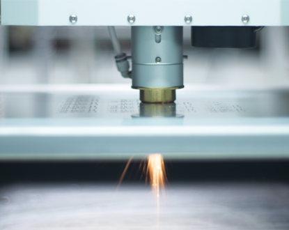 |
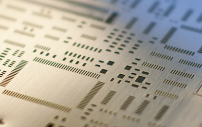
Laser Cutting SMT Stencils used a laser trimming to cut the features into a stainless steel plate in the desired shape, The main features of laser cut SMT stencils includes with high accuracy helps improve production efficiency and consistency, low cost and short production cycle,also with wide range of styles, suitable for various sizes of SMD components, as well as for pressure fitting and slurry discharge technologies. This method is suitable for various volume productions and PCB quick prototyping. |
|||||||||||
|
2, Prototype SMT Stencils : |
 |
Prototype SMT Stencils are manufactured also by laser cutting process, which soldering paste stencils do not have frames and are specifically created for manual printing purposes of quick turn around PCB orders, It is to save the time for PCB prototype assembly, to improves the quality of your prototype printed circuit boards assembly, And eliminates the monotonous and error-prone process of hand soldering your prototype PCBs. Prototype SMT stencils are tailored to your Gerber or CAD files in order to perfectly match your prototype printed circuit board. |
|||||||||||
|
3, Chemical Etching SMT Stencils : |
 |
Chemical Etching SMT Stencils are with main features of low cost and suitable for medium to large volume productions, Stable performance and suitable for multiple welding processes, And can be used for various sizes of SMD components and vertical components, but may not be suitable for very small sized elements, It used a photoresist process and an acid solution to form openings in the desired shape. This method is suitable for various volume productions. |
|||||||||||
|
Frame Sizes And Max Usable Area of Solder Paste Stencil : |
 |
|
Why Choose Panda PCB For SMT Stencils Services ? |
 |
Panda PCB Group offer our knowledge and experience of SMT Stencils Services to all of our PCB and PCBA customers, Our CAD experts combine industry designs and modification rules, honed by customer feedback and experimental development of PCB assembly, with your own specific design requirement and preference to produce SMT Stencils that are right the first time. We have our own SMT stencil CAD software, which allows us to accurately predict the transfer efficiency of paste/stencil aperture combinations and apply design rules to the stencil in order to optimize paste deposit repeatability, Customers just need to provide us the PCB paste file in panelization format (Gerber RS-274X, DXF,SVG ,EPS HPGL, AutoCad), We will select the suitable frame size to place the paste file to make the SMT Stencils used in the PCB assembly processes. |
SMT Stencils Thickness Recommendation: |
Laser Stencil Capabilities : |
|||||||||||||||||||||||||||||||||||||||
|
||||||||||||||||||||||||||||||||||||||||