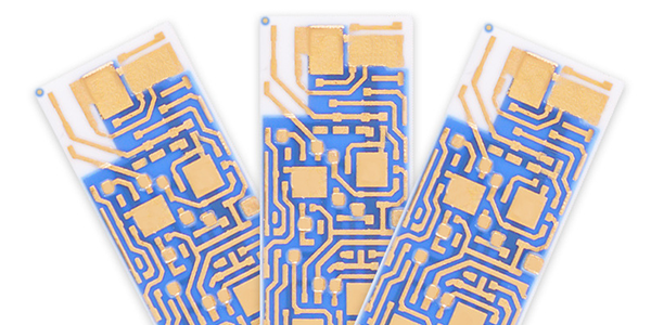
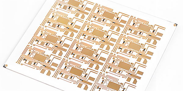
Thick Film Metallization Technology
Thick Film Metallization Technologies, also called Ceramic Metallization Technologies, are processes designed to apply conductive or resistive materials onto the surfaces of ceramic substrates, typically using mixtures of metal powders (such as gold, silver, or copper) and glass powders, which are screen-printed onto ceramic substrates like aluminum oxide (Al2O3) or aluminum nitride (AlN) before being subjected to high-temperature sintering to fuse the metal powders into stable conductive layers, enabling the creation of durable, high-performance circuits ideal for high-power, high-frequency applications in industries such as electronics, optoelectronics, and RF components.
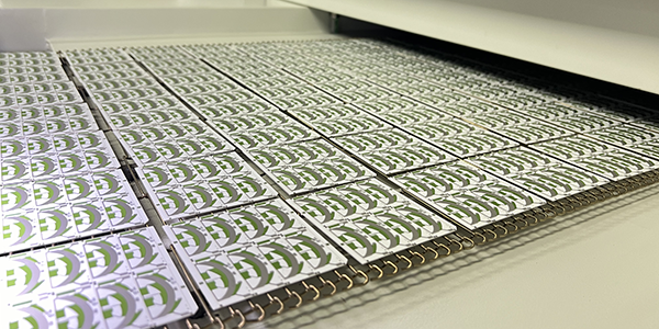
Thick Film Metallization Technologies rely on screen printing techniques to precisely apply conductive pastes made from metal and glass powders onto ceramic substrates. The pastes are then cured at temperatures typically ranging from 800°C to 1000°C, allowing the metal powders to form stable conductive layers and ensuring strong bonds between the metals and ceramics. The glass powders interact with the ceramic substrates during sintering, improving adhesion and long-term stability. This high-temperature process results in circuits that are highly stable and capable of withstanding harsh environments, which is critical for the reliability of electronic components.
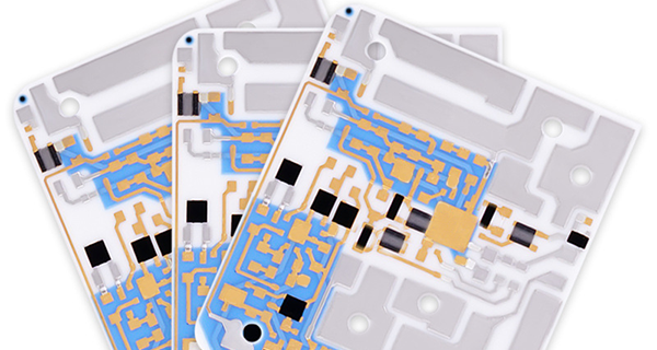
Ceramic Metallization Technologies are characterized by the ability to create high-density and high-reliability circuits. The screen printing methods allow for the easy construction of multilayer circuits, offering flexibility in circuit design. The sintering processes ensure exceptional thermal stability, wear resistance, and mechanical strength of the conductive layers. Additionally, these technologies provide precise control over the width and shape of circuits, which is essential for miniaturized and high-density designs. As a result, they are particularly suitable for high-power, high-frequency devices that require robust performance under challenging conditions.
Ceramic Metallization Technologies find widespread applications in high-performance electronic components, particularly in fields that demand high thermal resistance, electrical insulation, and stability under extreme conditions. Their applications span power electronics, optoelectronics, RF devices, and other high-reliability areas. These technologies are especially beneficial for components that operate under high temperatures and frequencies, where traditional wiring methods are not viable. The use of ceramic substrates ensures efficient performance in demanding environments, making Ceramic Metallization Technologies essential in the manufacturing of modern electronic devices.
Manufacturing of Thick Film Metallization Technology :
Thick Film Metallization Technologies are widely used electronic circuit manufacturing techniques for ceramic substrates, especially suitable for electronic devices that require high power, high frequency, high temperature, and high reliability. These technologies involve printing conductive materials (such as silver, gold, etc.) onto ceramic substrates, then sintering the materials to form circuit layers, and further achieving electrical connections and insulation protection. The key steps of these technologies are detailed below, following the order of the production processes.
1, Selection of Ceramic Substrate:
The ceramic substrate is the foundational material for thick film metallization technology. It not only needs to have good mechanical strength but also suitable thermal conductivity, electrical insulation, and a coefficient of thermal expansion (CTE) that matches the metal materials. Common ceramic substrate materials include:
● Alumina (Al2O3): A common and relatively low-cost material with good mechanical strength and heat resistance, suitable for general applications. Alumina substrates have low thermal conductivity but are sufficient for standard thick film circuits.
● Aluminum Nitride (AlN): Exhibits excellent thermal conductivity and electrical insulation, suitable for high power, high frequency, and high thermal management applications. Aluminum nitride has a low thermal expansion coefficient, which helps reduce thermal cycling stress.
● Titanium Dioxide (TiO2): Provides high insulation and strong thermal shock resistance, often used in special high-frequency or high-temperature applications.
When selecting a ceramic substrate, the material should be chosen based on the final product's performance requirements, such as thermal management, conductivity, and mechanical strength.
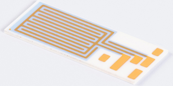
2, Screen Printing of Conductive Materials:
Printing the conductive layer onto the ceramic substrate surface is a core step in thick film metallization technology. Screen printing is used to create circuit patterns with conductive materials (such as silver, gold, silver-palladium alloy, gold-palladium alloy, copper, or carbon). Common conductive materials include:
● Silver: Known for its excellent conductivity, silver is widely used in most thick film circuits, particularly for low-cost products. However, silver's corrosion resistance is poor, making it unsuitable for extreme environments.
● Gold: Offers excellent conductivity and corrosion resistance, making it ideal for high-reliability, high-temperature applications, especially in aerospace or military equipment.
● Silver-Palladium Alloy (Ag/Pd): Combines the good conductivity of silver with the oxidation and corrosion resistance of palladium, making it suitable for high-frequency and high-temperature applications.
● Gold-Palladium Alloy (Au/Pd): Used in applications with high reliability requirements, providing stronger corrosion resistance and stability.
● Copper: Excellent conductivity and lower cost but requires additional protective layers (e.g., metal coating) due to copper's tendency to oxidize in air.
● Carbon: Used for specific circuit requirements, with lower conductivity, but it can be employed in resistors, sensors, and other components.
Screen printing technology ensures that conductive materials form the desired circuit pattern on the ceramic substrate. The viscosity and particle size of the ink are key factors in ensuring the accuracy of the printed pattern.
3, High-Temperature Sintering:
After screen printing, the conductive layer must be sintered at high temperatures to fix it to the ceramic substrate. The sintering temperature typically ranges from 850°C to 950°C. This process ensures strong adhesion between the conductive material and the ceramic substrate. Sintering helps to fuse the metal particles in the conductive material and remove any organic components, resulting in a conductive electrode layer with good conductivity, mechanical strength, and high-temperature resistance.
During the sintering process, the bond between the metal powder and the ceramic substrate strengthens, and a glass phase forms between the metal particles, further enhancing the interface strength between the electrode and the substrate.
4, Multilayer Circuits Interconnection:
As circuit complexity increases, multilayer interconnection technology becomes an important step in thick film metallization. This technology achieves higher circuit integration by using different conductive layers, dielectric layers, and interconnection materials.
● Via Conductor Filled Conductive Materials: To connect different layers electrically, vias are created in the ceramic substrate using laser or mechanical drilling technology. These vias are filled with conductive materials (such as silver paste or copper paste), forming conductive through-holes. These vias act as "bridges" to establish electrical connections between layers.
● Dielectric Layers: Typically made of ceramic materials (such as glass, alumina, or silica), dielectric layers are printed on top of each circuit layer to provide electrical insulation, mechanical strength, and thermal management.
● Circuits Cross-Over Technology: In multilayer circuits, line cross-over technology is used to connect lines from different layers. Precise design and processing ensure that electrical interconnections between layers are made without short circuits or interference.
5, Laser Trimming :
Laser trimming technology is used to make precise adjustments to the already sintered circuit, particularly for correcting resistors. By using a laser beam to cut or ablate the electrode material, the resistance value or linear characteristics can be precisely adjusted. This technology is not only applicable for adjusting the resistance value but also for fine-tuning other electrical parameters of the circuit to meet performance requirements.
Laser trimming is widely used in high-precision electronic products, allowing for precise control of each component's electrical performance without affecting other parts of the circuit.
6, High-Voltage Insulation Layer:
The high-voltage insulation layer is an essential protective measure to ensure the safe operation of thick film circuits in high-voltage applications. Typically, high-insulation materials (such as overglazes) are screen printed. After sintering, these materials provide the electrical isolation necessary for high-voltage conditions, preventing short circuits or current leakage.
The thickness and material selection of the insulation layer directly affect the circuit's high-voltage performance and long-term reliability. For certain special applications, additional protective treatments (such as sealing) may be needed to enhance the insulation layer's effectiveness.
7, Palladium-Gold Layer for Wire Bonding PADs:
In some high-end electronic products, gold wire bonding is a common method for connecting chips to ceramic substrates. To ensure good gold wire bonding, a palladium-gold layer is usually printed onto the bonding pads of the ceramic substrate.
● Palladium-Gold Printing: Palladium (Pd) has excellent oxidation resistance and good electrical conductivity, ensuring a long-lasting stable connection between the gold wire and the bonding pad. Screen printing technology can be used to apply a layer of palladium-gold onto the bonding pads, forming an appropriate bonding surface.
This selective printing technique ensures electrical performance while minimizing material waste. The use of palladium-gold is particularly important in high-frequency, high-reliability applications.
Thick Film Metallization Technologies involve several key process steps, with careful control at each stage directly affecting the final products' performance and reliability. From selecting the ceramic substrates to screen printing the conductive layers, sintering, multilayer interconnection, laser trimming, high-voltage insulation, and applying palladium-gold layers for wire bonding, each step ensures the stable operation of electronic devices in high-power, high-frequency, and extreme environments. With ongoing technological advancements, thick film metallization will continue to play vital roles in high-end electronics, power electronics, sensors, and other fields.
Applications of Thick Film Metallization Technology :
Thick Film Metallization Technologies are critical production processes for Ceramic PCBs, and they have found widespread applications in various electronic fields, especially in environments that require high power handling, high-frequency transmission, high-temperature resistance, or high mechanical strength. Below are some specific applications of thick film metallization technologies in various fields:
1. Power Electronics Devices:
Thick film metallization technology is extensively used in the manufacturing of power electronic devices, particularly in power conversion, power management, and drive systems. Thick film metallization forms highly conductive metal layers on ceramic substrates, which is crucial for components such as power switches (e.g., IGBT, MOSFET) and rectifiers. Since power electronics devices often need to handle high currents and voltages, the packaging materials must have excellent conductivity, thermal stability, and high voltage resistance.
● Power Modules: In power module packaging, thick film metallization is used to build electrical connection paths and heat dissipation paths, ensuring the system's stability and efficiency under high-power operation.
● Power Electronics Equipment: Used in power electronic systems for electric vehicles, power converters, etc.
2. Automotive Electronics:
The automotive electronics field has strict requirements for high reliability and durability of electronic devices. Due to its excellent temperature resistance and mechanical strength, thick film metallization technology has become an important technology in automotive electronics, particularly in in-vehicle controllers, sensors, and battery management systems (BMS). It can maintain stable electrical performance in high-temperature and harsh environments.
● Automotive Sensors: Thick film metallization technology is used in the electrodes and conductive paths of various automotive sensors, such as oil level sensors, throttle position sensors, temperature sensors, pressure sensors, and oxygen sensors.
● Battery Management Systems: Thick film metallization is used in the battery monitoring and control circuits of BMS systems to ensure stable operation in high-temperature and high-humidity environments.
● Power Drivers and Electronic Control Units: It provides reliable electrical connections and thermal management in automotive electronic systems.
3. Sensor Technology:
Thick film metallization technology is widely used in sensor applications, particularly in sensors for various physical quantities such as temperature, pressure, and gas concentration. Through thick film metallization, sensors not only achieve precise electrical connections but also ensure high-temperature resistance and interference immunity.
● Oxygen Sensors: Used in automotive exhaust treatment systems and industrial emission monitoring, thick film metallization technology is employed to manufacture the electrodes of oxygen sensors.
● Temperature Sensors: In automotive, industrial equipment, and medical devices, temperature sensors require fast response and stability, and thick film technology provides a stable conductive layer to ensure sensor accuracy and durability.
● Pressure Sensors: Widely used in the manufacture of pressure sensor electrodes and conductive paths, these sensors are common in industrial automation, aerospace, and automotive applications.
4. Radio Frequency and Microwave Components:
Thick film metallization technology plays an important role in high-frequency applications, particularly in the manufacture of RF and microwave components. It not only ensures good conductivity but also effectively reduces high-frequency signal losses, improving device performance.
● RF Filters and Antennas: In communication devices, radar, and satellite communication systems, RF components require stable electrical performance and efficient signal transmission. Thick film metallization technology is used in the electrodes, conductors, and connectors of RF circuits.
● Microwave Circuits: Used in microwave circuit fabrication, thick film metallization ensures signal integrity and transmission efficiency.
5. High-Temperature Environment Applications:
Thick film metallization technology is especially suitable for electronic applications in high-temperature environments. The metal layer formed during the sintering process can create a very stable and high-melting-point metal structure, which maintains good electrical conductivity even under high-temperature conditions.
● Aerospace: In the aerospace field, thick film metallization is used in satellites, power systems, and engine control systems to ensure reliable operation in extreme temperatures.
● Industrial Equipment: Thick film metallization is applied in high-temperature sensors and power control modules, improving the stability and lifespan of devices working in high-temperature environments.
6. Integrated Circuit Packaging:
In integrated circuit (IC) packaging, thick film metallization technology is widely used in the manufacturing of multi-layer circuit boards (MLB) or substrates. It provides stable electrical connections and thermal management, particularly in high-power, high-density packaging.
● High-Density Integrated Circuit Packaging: Thick film metallization is used in the manufacturing of high-density circuit boards, enabling miniaturization, lightweight design, and efficient electrical connections.
● Multi-Chip Modules: For modules integrating multiple chips, thick film metallization provides reliable electrical and thermal connections, supporting complex system integration.
7. Medical Electronics:
In medical electronic devices, especially implantable devices such as pacemakers and sensors, thick film metallization technology provides stable electrical connections and ensures long-term reliability inside the human body. Additionally, these devices need to be resistant to high temperatures, corrosion, and the invasion of bodily fluids, all of which are requirements met by thick film metallization.
● Implantable Medical Devices: For devices like heart pacemakers and brain stimulators, thick film metallization is used for electrical connections and battery management systems.
● Medical Sensors: Sensors used in vital sign monitoring, such as blood glucose monitoring sensors, use thick film metallization to achieve precise electrical connections and signal processing.
8. Photovoltaic and Energy Applications:
With the rise of new energy technologies, thick film metallization technology is increasingly important in solar photovoltaic panels and other energy management systems. Thick film technology is used in the electrode layers of photovoltaic components, ensuring the conductivity and long-term reliability of solar cells.
● Solar Panels: Thick film metallization is used in the electrode layers of photovoltaic modules, helping to achieve efficient energy conversion and stable long-term performance.
● Energy Storage Devices: Thick film metallization technology can also be applied in the connections of battery management systems and electrode materials in devices like lithium batteries and supercapacitors.
Ceramic Metallization Technologies have a wide range of applications in modern electronics, from power electronics to sensors, RF communication, and medical devices. They provide stable and reliable solutions across industries. As technologies advance, thick film metallization will continue to drive innovation, especially in devices that operate under high power, high frequency, and high-temperature conditions, demonstrating their irreplaceable advantages.
For more information, Please refer to Thick Film Substrates.
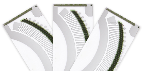
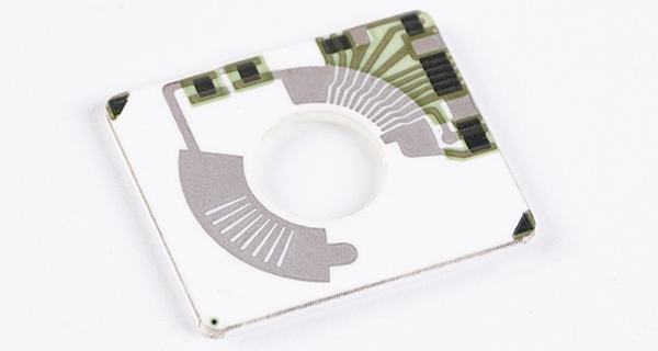
Custom Thick Film Sensors
- Custom Thick Film Sensor Elements
- Fuel Level Sensor PCB
- Fuel Level Sensor Ceramic PCB
- Oil Level Sensor Ceramic PCB
- Motorcycle Fuel Level Sensor PCB
- Throttle Position Sensor PCB
- Throttle Position Sensor FR4 PCB
- Throttle Position Sensor Ceramic PCB
- Throttle Position Sensor Flexible PCB
- Accelerator Pedal Sensor PCB
- Accelerator Pedal Position Sensor PCB
- Pedal Position Sensor Carbon PCB
- Potentiometer PCB
- Linear Potentiometer Carbon Track PCB
- Rotary Potentiometer Carbon Track PCB
- FR4 Potentiometer Carbon PCB
- Ceramic Potentiometer Carbon PCB
- Flexible Potentiometer Carbon PCB
- Logarithmic Taper Potentiometer PCB
- Position Sensor PCB
- FR4 Position Sensor Carbon PCB
- Ceramic Position Sensor Carbon PCB
- Flexible Position Sensor Carbon PCB
- Flexible Sensor PCB
- Printed Flexible Electronic PCB
- Printed Carbon PCB
- Ceramic Pressure Sensors
- Ceramic Thick Film Pressure Sensors
- Engine Oil Pressure Sensor PCB
- Gold Coated Ceramic Substrates
- Gold Coated Thick Film Substrates
- Metallized Ceramic Substrates
- Multilayer Thick Film Substrates
- Thick Film Metallization Technology
- Thin Film Metallization Technology
- Thin Film Ceramic PCB
- Variable Resistor Carbon PCB
- Remote Ready Sender Ceramic PCB
- LP Gas Tank Gauges Ceramic PCB
- Thick Film Capacitive Sensors
- Thick Film Capacitive Pressure Sensors
- Thick Film Edible Oil Quality Sensors
- Thick Film Meteorological Rainfall Sensors
- PI Interdigital Electrodes (Flexible)
- Air Door Actuator PCB
- HVAC Blend Door Actuator PCB