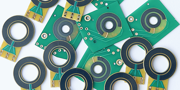
Printed Carbon PCB
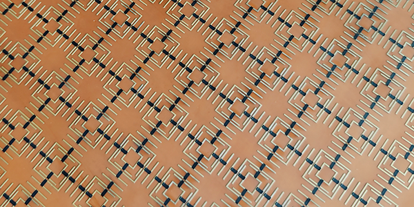
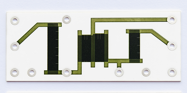
Printed Carbon PCBs, also called Carbon Ink PCBs, are a specialized type of printed circuit board that uses conductive carbon ink to create circuits on a substrate through screen printing or inkjet printing techniques, enabling the formation of conductive paths that can perform multiple functions, including interconnections, resistors, switch contacts, and electromagnetic shielding, making them ideal for low-power electronic applications, particularly where space and flexibility are important.
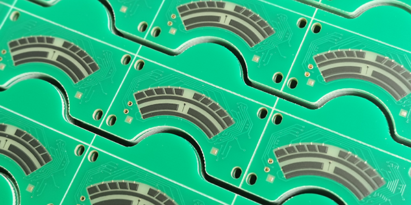
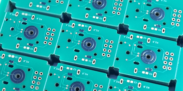
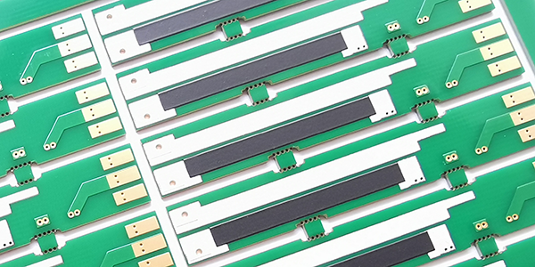
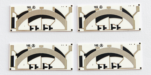
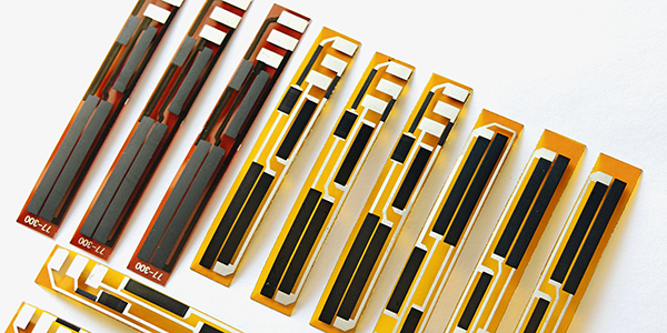
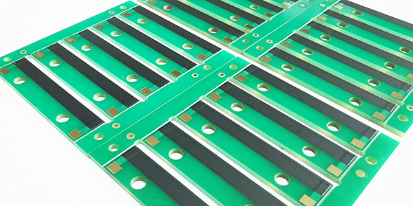
Printed Carbon PCBs are produced through a multi-step process, starting with the selection of a suitable substrate, such as polyimide, FR-4, or ceramic, chosen for their electrical and mechanical properties. Conductive carbon ink is then applied using screen or inkjet printing to form precise conductive patterns. Afterward, the PCB is dried and cured to stabilize the ink's conductivity. Finally, insulating layers or encapsulation may be added to enhance the board’s durability and functionality.
Carbon Ink PCBs feature reliable conductivity, making them ideal for low-power electronic applications. Their flexibility allows them to be molded into various shapes, while their lightweight nature suits applications where weight is critical. The manufacturing process is environmentally friendly, using fewer harmful chemicals, and these boards are cost-effective for mass production. Additionally, they are durable, withstanding over 100,000 keystrokes or 5 millions of sensor life cycles without performance degradation.
Printed Carbon PCBs are widely used, especially in low-power electronic products. They are commonly found in products such as televisions, telephones, electronic keyboards, game consoles, and video recorders. Additionally, printed carbon PCBs are an ideal choice for flexible electronic, pressure sensors, high voltage resistors, heating elements, position sensors, and temperature sensors, where the combination of flexibility and conductivity is crucial. Carbon Ink PCBs are also used in emerging technologies such as wearable devices, smart home products, and medical instruments, where compact size, energy efficiency, and reliable performance are essential factors.
Applications of Printed Carbon PCB :
● Low-Power Electronic Products: In products such as televisions, phones, electronic keyboards, game consoles, and video recorders, carbon PCBs enhance circuit connections and functionality due to their good conductivity and cost-effectiveness.
● Computers and Office Equipment: Devices like computer keyboards and card-based computers use carbon PCBs to meet the demand for low cost and high reliability.
● Audio and Measurement Equipment: Miniature recorders and electronic measuring instruments extensively use carbon PCBs due to their lightweight and thin profile.
● Conductive Rubber Keyboards: In industrial control and consumer electronics (like TV remotes and garage door controllers), carbon PCBs support the functionality of conductive rubber keyboards, improving tactile response.
● RF Shielding and Automotive Electronics: Carbon PCBs are widely applied in keyboards, remote controls, automotive controls, industrial engines, and welding equipment where RF shielding is required.
● Communication Devices: Mobile phones, televisions, wireless routers, and base stations utilize carbon PCBs for connections and data transmission between electronic components.
● Computer Hardware: Components like motherboards, graphics cards, and memory modules rely on carbon PCBs for electrical connections and structural support, ensuring signal transmission and exchange.
● Consumer Electronics: In products such as smartphones, tablets, and wearables, carbon PCBs ensure electrical connections, signal transmission, and power management, enhancing product performance.
● Industrial Control Systems: Used in industrial control applications like potentiometers and linear position sensors.
● Wearable Devices: Due to their flexibility and lightweight design, carbon PCBs are suitable for wearable technologies like smartwatches and fitness trackers.
● Sensors and Smart Homes: Widely applied in environmental monitoring, health monitoring, and smart home applications, accommodating various shapes and design needs.
● Flexible Electronics: Can be used in flexible displays and electronic tags, supporting complex structures.
● Medical Devices: Help achieve real-time monitoring in wearable health monitoring devices and portable diagnostic tools.
● Automotive Electronics: Used in throttle position sensors, pedal sensors, and touch sensors and switches for automotive interiors and control panels.
Main Features of Carbon Ink PCB :
● Flexibility: Carbon Ink PCBs offer excellent flexibility, allowing them to adapt to bending and irregular shapes, making them ideal for applications in wearable devices, sensors, and flexible electronics.
● Low Cost: Compared to traditional copper foil circuit boards, the manufacturing cost of Carbon Ink PCBs is lower because the carbon ink material is inexpensive and easy to print, making it suitable for mass production.
● Environmental Friendliness: The carbon ink materials used are generally non-toxic, harmless, and biodegradable, complying with environmental requirements and promoting sustainable development.
● Electromagnetic Shielding: The carbon ink layer provides good electromagnetic shielding properties, effectively reducing electromagnetic interference and enhancing circuit stability.
● Wear Resistance: Carbon Ink PCBs exhibit outstanding durability, capable of withstanding over 1 million key presses and 5 million sliding operations (for potentiometers), demonstrating excellent wear resistance.
● Adhesion Stability: The circuit surface must have good adhesion stability, suitable for warm climates, ensuring even coverage.
● Alignment Tolerance: The minimum overlap width (footprint) of carbon coverage over copper lines is 0.2 mm, ensuring circuit reliability and production feasibility.
● Line Width and Spacing: The minimum carbon ink line width is 0.25 mm, with a minimum spacing of 0.2 mm and a standard thickness of 15 µm.
● Resistance Value: The typical resistance value tolerance is +/-10%, with laser trimming tolerance reaching +/-1.0%, and linearity <1.0% (for potentiometers or position sensors).
● Conductivity: Carbon ink possesses high conductivity, meeting the needs of general electronic circuits and suitable for low-power electronic products.
● Lightweight Design: Carbon Ink PCBs are relatively lightweight, making them suitable for electronic devices with strict weight requirements, such as smart home products and wearable devices.
● Wide Applications: They are applicable in various fields such as electronic devices, sensors, and medical equipment, particularly suitable for low-power applications.
Carbon Ink PCBs have gained widespread favor in the modern electronics industry due to their comprehensive advantages, particularly in response to the growing demand for flexible circuits and environmental sustainability. These features provide Carbon Ink PCBs with notable benefits in cost-effectiveness, flexibility, and environmental friendliness, making them well-suited for a wide range of electronic applications.
Process Capabilities of Printed Carbon PCB :
Items |
Typical Values |
1, Substrates : |
FR4, Alumina (Ceramic), Polyimide (Flexible PCB), Stainless Steel (SUS304), Mica |
2, Conductors Material : |
Copper, Silver , Gold , Silver-Palladium, Palladium-Gold |
3, Thick Film Carbon Thickness (height) : |
15um +/-5 um |
4, Silver Palladium Thickness (height) : |
12um+/-5um |
5, Minimum Width of Thick Film Traces : |
0.25 mm +/-0.05 mm |
6, Minimum Spacing of Thick Film Traces : |
0.25 mm +/-0.05 mm |
7, Minimum Footprint (Carbon to Copper) : |
No less than 0.20mm |
8, Sheet Resistivity (ohms/square): |
Printed resistors in milli ohm to mega ohm range (Customizable) with tolerances of 1-10% are fabricated and protected with overglaze materials |
9, Resistor Value Tolerance : |
+/-10.0% (Standard) (Customizable) |
10, Linearity : |
+/-1.0% (Standard) (Customizable) |
11, Synchronism of Potentiometers (Double Channels) : |
+/-2.0% (Standard) (Customizable) |
12, Durability of Carbon Ink (Life time) : |
0.5 Million (Min), 2.0-5.0 Million (Standard) |
13, Working Temperature : |
- 40℃ /+150℃ |
For more information, Please refer to Thick Film Resistor PCB.
Custom Thick Film Sensors
- Custom Thick Film Sensor Elements
- Fuel Level Sensor PCB
- Fuel Level Sensor Ceramic PCB
- Oil Level Sensor Ceramic PCB
- Motorcycle Fuel Level Sensor PCB
- Throttle Position Sensor PCB
- Throttle Position Sensor FR4 PCB
- Throttle Position Sensor Ceramic PCB
- Throttle Position Sensor Flexible PCB
- Accelerator Pedal Sensor PCB
- Accelerator Pedal Position Sensor PCB
- Pedal Position Sensor Carbon PCB
- Potentiometer PCB
- Linear Potentiometer Carbon Track PCB
- Rotary Potentiometer Carbon Track PCB
- FR4 Potentiometer Carbon PCB
- Ceramic Potentiometer Carbon PCB
- Flexible Potentiometer Carbon PCB
- Logarithmic Taper Potentiometer PCB
- Position Sensor PCB
- FR4 Position Sensor Carbon PCB
- Ceramic Position Sensor Carbon PCB
- Flexible Position Sensor Carbon PCB
- Flexible Sensor PCB
- Printed Flexible Electronic PCB
- Printed Carbon PCB
- Ceramic Pressure Sensors
- Ceramic Thick Film Pressure Sensors
- Engine Oil Pressure Sensor PCB
- Gold Coated Ceramic Substrates
- Gold Coated Thick Film Substrates
- Metallized Ceramic Substrates
- Multilayer Thick Film Substrates
- Thick Film Metallization Technology
- Thin Film Metallization Technology
- Thin Film Ceramic PCB
- Variable Resistor Carbon PCB
- Remote Ready Sender Ceramic PCB
- LP Gas Tank Gauges Ceramic PCB
- Thick Film Capacitive Sensors
- Thick Film Capacitive Pressure Sensors
- Thick Film Edible Oil Quality Sensors
- Thick Film Meteorological Rainfall Sensors
- PI Interdigital Electrodes (Flexible)
- Air Door Actuator PCB
- HVAC Blend Door Actuator PCB