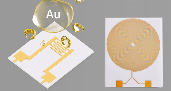
Metallized Ceramic Substrates
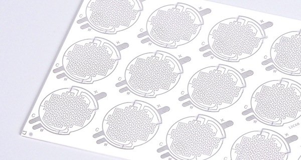
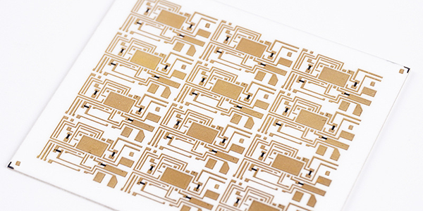
Metallized Ceramic Substrates, also called Metallized Ceramic Sensors, are electronic components featuring a conductive metal layer applied to the surface of a ceramic substrate through thick-film printing or thin-film deposition processes, with the metal layer, typically made from conductive materials such as silver, copper, or gold, used to create circuits or interconnections for electronic devices, and metallized ceramic substrates offer high thermal conductivity, excellent mechanical strength, and resistance to high temperatures, making them ideal for supporting high-power electronic components.
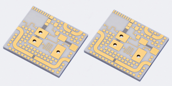
Metallized Ceramic Substrates combine the insulating properties of ceramics, such as alumina or aluminum nitride, with the conductivity of metals, creating a robust platform for high-performance electronic components. These substrates offer excellent thermal conductivity, which aids in efficient heat dissipation, enhancing the longevity and reliability of electronic products. In addition to their superior thermal management, metallized ceramic substrates also provide high mechanical strength and electrical insulation, ensuring stable circuit connections and protecting electronic systems from short circuits or interference.
Metallized Ceramic Sensors are widely used in demanding applications such as power modules, LED lighting, and power electronics, which operate under high-frequency, high-power, and high-temperature conditions. Their unique combination of thermal management and electrical properties makes them essential in power electronics, high-frequency circuits, and automotive electronics. These substrates play a critical role in improving the performance and reliability of electronic systems, ensuring they function efficiently in a variety of high-performance environments.
Process Types of Metallized Ceramic Substrates :
1. Thick Film Metallization Technology :
Thick film metallization typically involves applying a metal paste (which includes conductive or resistive materials) onto the surface of the ceramic substrate, followed by a sintering process to bond the metal to the substrate. The sintering temperature is relatively high, usually between 800°C and 1000°C. The thickness of the metal layer is typically between 10 microns and 100 microns.
Technical Characteristics:
● Thicker Metal Layer: The metal layer is thicker, offering higher current carrying capacity, suitable for high-power and high-current applications.
● Simpler Process: Compared to thin film technology, the thick film process is simpler, making it more suitable for large-scale production.
● Lower Cost: Because the process is relatively simple and the raw materials are inexpensive, it is suitable for cost-sensitive applications.
Advantages:
● High Current Carrying Capacity: The thicker metal layer can handle higher current loads.
● Stronger Adaptability: Thick film metallization requires lower-quality substrates, allowing for less precise ceramic surfaces, thus simplifying production.
● Lower Cost: Compared to thin film processes, thick film technology typically has lower production costs.
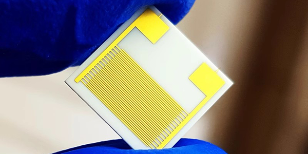
2. Thin Film Metallization Technology :
Thin film metallization involves using techniques such as Physical Vapor Deposition (PVD) or Chemical Vapor Deposition (CVD) to precisely deposit metal materials onto the ceramic substrate in the form of a thin film. This process usually takes place at lower temperatures, allowing for the deposition of metal layers with precise thickness and uniformity. The metal layer is typically much thinner, usually a few microns.
Technical Characteristics:
● Thinner Metal Layer: The metal layer is thin and uniform, offering good electrical conductivity and stability.
● High Precision: Thin film technology allows for the creation of very precise circuit patterns, making it suitable for applications requiring high precision and density.
● Material Flexibility: A variety of materials (such as gold, aluminum, copper, etc.) can be used for deposition, meeting the needs of different applications.
Advantages:
● High Precision and Density: Thin film technology enables the production of finer circuit patterns and structures, making it suitable for high-precision and high-density applications.
● Good Thermal Stability: Thin film metallization tends to offer better thermal stability, making it suitable for environments with high thermal demands.
● Smooth Surface: The metal layer is uniformly thin and the surface is smooth, which is beneficial for high-frequency and high-speed applications.
Manufacturing of Metallized Ceramic Substrates :
1, Ceramic Substrate Production: The base material is usually made from high-purity ceramics like alumina (Al203), aluminum nitride (AlN), or beryllium oxide (BeO). These ceramics are selected for their excellent thermal and electrical insulating properties.
2, Metallization: The ceramic surface is coated with a metal layer. This is commonly achieved through methods such as:
● Thick Film Printed Circuits and Sintering: The substrate and metal layer are subjected to high temperatures to bond the metal to the ceramic effectively, the main conductive materials can be Silver, Palladium-Silver or Gold, Palladium-Gold.
● Physical Vapor Deposition (PVD): This technique involves depositing (Copper) metal in a vacuum environment to form a thin, uniform layer.
● Chemical Vapor Deposition (CVD): Metal (Copper) is deposited from gaseous precursors onto the ceramic surface.
● Electroless Plating: Metal (Copper) is deposited onto the ceramic substrate through a chemical reaction without the use of electrical current.
● Patterning: In cases where specific circuit patterns are needed, additional processes such as photolithography are used to define the metal layer’s structure.
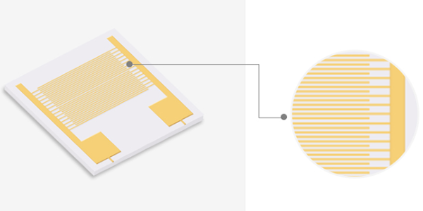
These metallization processes can involve various techniques such as Thin Film or Thick Film Hybrid Circuits, Sputtering, Electroplating, Chemical Vapor Deposition, and thermal evaporation, each serving different needs in terms of metal layer thickness and application requirements.
Performances of Metallized Ceramic Sensors :
Metallized Ceramic Sensors exhibit exceptional thermal conductivity, crucial for heat dissipation in high-power applications. The metal layer also ensures high electrical conductivity, improving signal transmission and reducing losses, particularly in high-frequency applications. Metallized ceramic substrates offer several important properties:
● Electrical Insulation: The ceramic material provides excellent electrical insulation, preventing electrical interference and short circuits.
● Thermal Conductivity: Ceramics used in these substrates often have high thermal conductivity, which helps dissipate heat generated by electronic components.
● Mechanical Strength: The ceramic base is generally strong and durable, supporting various electronic components and protecting them from mechanical damage.
● Thermal Expansion Compatibility: The metal layer and ceramic base are designed to have compatible thermal expansion coefficients to prevent warping or cracking during thermal cycling.
Advantages of Metallized Ceramic Sensors :
Key advantages of Metallized Ceramic Sensors include great heat conductivity and temperature resistance, high insulation voltage, and a low coefficient of thermal expansion that outperforms substrates based on metal or plastic. The metallization process enhances the substrate's mechanical strength and durability, providing additional protection against mechanical stress, Please check the main advantages as follows:
● High Thermal Conductivity: The ceramic substrate efficiently conducts heat away from sensitive electronic components, enhancing reliability and performance.
● Electrical Insulation: The ceramic base provides excellent insulation, making it ideal for high-voltage applications.
● Durability: The combination of metal and ceramic offers robust mechanical strength and resistance to environmental factors such as moisture and chemicals.
● Design Flexibility: Metallized Ceramic Sensors can be tailored to specific requirements, including various metal patterns and substrate sizes.
● Improved Performance: Due to their excellent thermal management and electrical insulation properties, metallized ceramic substrates help improve the overall performance and longevity of electronic devices.
Applications of Metallized Ceramic Substrates :
Metallized Ceramic Substrates (Metallized Ceramic Sensors) have a wide range of applications due to their unique properties such as high thermal conductivity, mechanical strength, and resistance to high temperatures. Some key applications include:
● Power Electronics: Metallized ceramic substrates are widely used in power electronic devices like power transistors, diodes, and thyristors. Their high thermal conductivity helps dissipate the heat generated by these components, allowing them to function at higher power levels.
● LED Lighting: In high-performance LED lighting systems, metallized ceramic substrates are used to mount LED chips. They help in efficient heat dissipation, extending the life of the LEDs and improving performance.
● Automotive Electronics: These substrates are commonly used in automotive systems, including in sensors, control units, and power modules. The durability and temperature resistance of metallized ceramic substrates make them ideal for use in harsh automotive environments.
● Telecommunications: Metallized ceramic substrates are used in the production of microwave components, such as filters, antennas, and passive circuit elements. They help maintain signal integrity and manage heat in these high-frequency applications.
● Industrial Equipment: They are used in industrial applications such as power supplies, motor control, and other high-power devices, where their strength and thermal properties are critical for reliable performance in demanding environments.
● Medical Devices: In medical electronics, such as pacemakers and diagnostic equipment, metallized ceramic substrates are used for their biocompatibility, stability, and heat management capabilities.
● Sensors and Actuators: Metallized ceramic sensors are used in various sensing applications, including temperature, pressure, and gas sensing. They provide precise and stable readings in harsh environments due to their robust mechanical and thermal properties.
In power electronics, Metallized Ceramic Substrates are crucial for circuits that operate under high-frequency, high-power, and high-temperature conditions, enabling reliable performance in demanding environments. Additionally, they are commonly used in automotive electronics, where durability and thermal stability are essential for components such as inverters, sensors, and power control units. Their ability to maintain stable electrical connections while withstanding high stress and temperatures makes them indispensable in sectors such as aerospace, industrial machinery, and renewable energy systems. Overall, metallized ceramic substrates are key to enhancing the efficiency, reliability, and longevity of a wide range of advanced electronic systems.
Future of Metallized Ceramic Substrates :
The future of Metallized Ceramic Substrates (Metallized Ceramic Sensors) looks promising due to continuous advancements in materials science and the growing demand for high-performance electronic devices. Several factors indicate the direction in which these substrates are heading:
● Miniaturization and High-Density Packaging: As electronics become more compact, the need for smaller, more efficient components grows. Metallized ceramic substrates are well-suited for miniaturization due to their ability to handle high power levels in smaller form factors. This will drive their use in high-density packaging for both consumer electronics and industrial applications.
● Improved Thermal Management: As devices become more powerful, the demand for better heat dissipation increases. Metallized ceramic substrates will continue to evolve with improvements in thermal conductivity and heat resistance, addressing the growing need for efficient thermal management in applications like power electronics, electric vehicles (EVs), and renewable energy systems.
● Electric Vehicles and Green Technologies: The shift toward electric vehicles (EVs) and renewable energy technologies is expected to create significant demand for advanced electronic components. Metallized ceramic substrates, with their excellent thermal and mechanical properties, will be integral in the development of power electronics for EVs, energy storage systems, and renewable energy converters.
● Integration with IoT and Smart Devices: The rise of the Internet of Things (IoT) and smart devices will drive the need for more advanced sensors and actuators. Metallized ceramic sensors will play a key role in various IoT applications, particularly in harsh or high-temperature environments, where traditional electronic components may not be suitable.
● Advanced Materials: Ongoing research into new ceramic materials, such as advanced oxide and nitride ceramics, will further enhance the performance of metallized ceramic substrates. These materials could offer better conductivity, higher temperature resistance, and more efficient heat dissipation, making them even more valuable in cutting-edge electronics.
● Cost Reduction and Scalability: With advancements in manufacturing techniques and economies of scale, the production cost of metallized ceramic substrates is expected to decrease, making them more accessible for a wider range of applications. This will expand their adoption in industries like consumer electronics, telecommunications, and medical devices.
● Sustainability and Eco-Friendly Manufacturing: As the global focus shifts towards sustainability, there will be an increased demand for eco-friendly and recyclable electronic components. Metallized ceramic substrates, being made from inorganic materials, are inherently more environmentally friendly compared to other alternatives, making them a good fit for green manufacturing practices.
Optional Processes of Metallized Ceramic Substrates :
Items |
Thick Film Capabilities |
DCB/DBC Capabilities |
DPC Capabilities |
AMB Capabilities |
Layer Counts |
2, 4, 6, 10 Layers |
2 Layers |
2 Layers |
2 Layers |
Max Board Dimension |
200*200mm |
138*178mm |
138*190mm |
114*114mm |
Min Board Thickness |
0.25mm |
0.30mm~0.40mm |
0.25mm |
0.25mm |
Max Board Thickness |
2.0mm |
1L: 1.3mm; 2L 1.6mm |
2.0mm |
1.8mm |
Conductor Thickness |
5um - 15um |
1.0oz - 9.0oz |
20um - 200um |
1oz- 22oz |
Min Line Width/Line Space |
6/8mil (0.15/0.20mm) |
12/12mil (0.30/0.30mm) |
6/8mil (0.15/0.20mm) |
20/20mil (0.50/0.50mm) |
Substrates Type |
AI203, ALN, BeO, ZrO2 |
AI203, ALN, ZrO2 |
AI203, ALN, ZrO2, Si3N4 |
ALN, Si3N4 |
Min Hole Diameter |
4mil (0.1mm) |
4mil (0.1mm) |
4mil (0.1mm) |
4mil (0.1mm) |
Outline Tolerance |
Laser: +0.2/0.05mm; |
Laser: +0.2/0.05mm; |
Laser: +0.2/0.05mm; |
Laser: +0.2/0.05mm; |
Substrate Thickness |
0.25, 0.38, 0.50, 0.635, 0.80,1.0, 1.25, 1.5, 2.0mm, Also can be customized |
0.25, 0.38, 0.50, 0.635, 0.76,1.0mm |
0.25, 0.38, 0.50, 0.635, 0.80, |
0.25, 0.38, 0.50, 0.635, 0.76,1.0mm |
Surface Treatment |
AgPd, AuPd, Mn/Ni |
OSP/Ni Plating, ENIG |
OSP/ENIG/ENEPIG |
OSP/Ni Plating, ENIG |
Min Solder PAD Dia |
10mil (0.25mm) |
8mil (0.20mm) |
6mil (0.15mm) |
8mil (0.20mm) |
For more information, Please refer to Ceramic PCB.
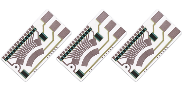
Custom Thick Film Sensors
- Custom Thick Film Sensor Elements
- Fuel Level Sensor PCB
- Fuel Level Sensor Ceramic PCB
- Oil Level Sensor Ceramic PCB
- Motorcycle Fuel Level Sensor PCB
- Throttle Position Sensor PCB
- Throttle Position Sensor FR4 PCB
- Throttle Position Sensor Ceramic PCB
- Throttle Position Sensor Flexible PCB
- Accelerator Pedal Sensor PCB
- Accelerator Pedal Position Sensor PCB
- Pedal Position Sensor Carbon PCB
- Potentiometer PCB
- Linear Potentiometer Carbon Track PCB
- Rotary Potentiometer Carbon Track PCB
- FR4 Potentiometer Carbon PCB
- Ceramic Potentiometer Carbon PCB
- Flexible Potentiometer Carbon PCB
- Logarithmic Taper Potentiometer PCB
- Position Sensor PCB
- FR4 Position Sensor Carbon PCB
- Ceramic Position Sensor Carbon PCB
- Flexible Position Sensor Carbon PCB
- Flexible Sensor PCB
- Printed Flexible Electronic PCB
- Printed Carbon PCB
- Ceramic Pressure Sensors
- Ceramic Thick Film Pressure Sensors
- Engine Oil Pressure Sensor PCB
- Gold Coated Ceramic Substrates
- Gold Coated Thick Film Substrates
- Metallized Ceramic Substrates
- Multilayer Thick Film Substrates
- Thick Film Metallization Technology
- Thin Film Metallization Technology
- Thin Film Ceramic PCB
- Variable Resistor Carbon PCB
- Remote Ready Sender Ceramic PCB
- LP Gas Tank Gauges Ceramic PCB
- Thick Film Capacitive Sensors
- Thick Film Capacitive Pressure Sensors
- Thick Film Edible Oil Quality Sensors
- Thick Film Meteorological Rainfall Sensors
- PI Interdigital Electrodes (Flexible)
- Air Door Actuator PCB
- HVAC Blend Door Actuator PCB