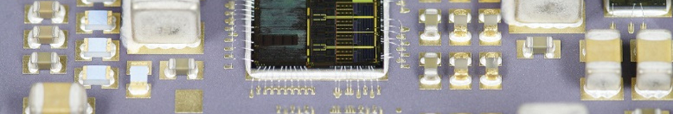
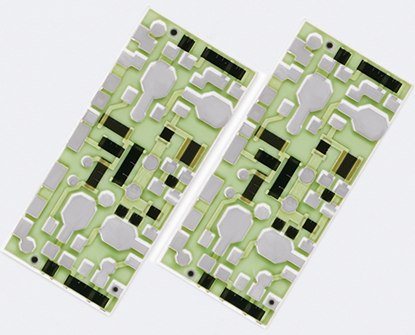
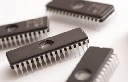
Hybrid Integrated Circuits
Hybrid Integrated Circuits, also called Hybrid Circuits, are compact electronic circuits manufactured using thick film technology combined with ceramic substrates, integrating both passive components, such as resistors and capacitors, and active components, such as transistors and diodes, into a single package to enhance performance and functionality across various applications, offering several advantages over traditional printed circuit boards, including higher component density, superior reliability, and customization for specific application requirements, making them ideal for demanding environments like aerospace, automotive, telecommunications, and military systems. Hybrid Integrated Circuits are also a type of electronic circuit that combines multiple components on one substrate, typically ceramic or quartz. It consists of a combination of miniature passive and active electronic components like resistors, capacitors, transistors, diodes, and inductors that are mounted onto a single package by using small metallic wires or conductive pathways to connect them together. Hybrid Circuits typically involve the integration of discrete components onto a substrate using thick film or thin technology. These hybrid integrated circuits are used in a wide range of applications including telecommunications, military, aerospace, medical, automotive, and consumer electronics, due to their compact size, low power consumption, high reliability, and cost-effectiveness. Features of Hybrid Integrated Circuits : |
 |
|
 |
1, High Reliability: Hybrid Integrated Circuits are highly reliable due to the use of hermetically sealed packages and the ability to test each component before assembly. This ensures that any defective components are eliminated before final assembly. 2, High Density: Hybrid Circuits use thin-film or thick-film technology to achieve a high component density on a small substrate. This makes them ideal for miniaturized electronic systems. 3, Customizable: Hybrid Integrated Circuits can be customized for specific applications by selecting the appropriate components and layout. This allows for optimal performance and cost effectiveness. |
|
4, Wide Range of Applications: Hybrid Integrated Circuits are used in a wide range of applications such as aerospace, military, medical, automotive, telecommunications, and consumer electronics. 5, Improved Performance: Hybrid Integrated Circuits can offer better performance compared to traditional circuits due to their compact size and the ability to integrate both analog and digital circuits. 6, Low Power Consumption: Hybrid Circuits consume less power than traditional circuits due to their small size and efficient design. Please refer to Thick Film Technology for more informations. |
||
Advantages of Hybrid Integrated Circuits : |
Hybrid Integrated Circuits combine the advantages of both monolithic and discrete circuits while offering additional benefits. Here are some of the main advantages of hybrid integrated circuits: 1, Miniaturization: Hybrid integrated circuits enable miniaturization of electronic systems by integrating multiple components on a small substrate. This reduction in size is particularly valuable in portable devices, aerospace applications, and any other scenario where space is limited. |
|
 |
2, Component Integration: Hybrid integrated circuits allow for the integration of various components, such as resistors, capacitors, inductors, diodes, transistors, and even microprocessors, on a single substrate. This integration reduces the overall size and complexity of the circuit, making it more compact and efficient. 3, Reliability: Hybrid circuits are known for their high reliability. The use of hermetically sealed packages and rigorous testing during assembly ensures that each component is functioning properly. This eliminates defective components before final assembly, leading to increased reliability and product longevity. 4, Cost-Effectiveness: Although Hybrid integrated circuits may have higher upfront costs due to the complexity of manufacturing and assembly processes, they can result in cost savings in the long run. The integration of multiple components on a single substrate reduces the need for additional external components, simplifies assembly, and enhances overall system efficiency. |
5, Customizability: Hybrid circuits offer a high degree of customizability, allowing for the design and implementation of circuits tailored to specific applications. The ability to select and integrate different components and technologies enables HICs to meet specific performance, power, and size requirements. 6, Low Power Consumption: With the integration of various components and optimized circuit design, Hybrid Integrated Circuits can offer reduced power consumption compared to traditional circuits. This is especially important in battery-powered devices, where energy efficiency is crucial. 7, High Performance: Hybrid integrated circuits can achieve high levels of performance due to the ability to integrate both analog and digital functions on the same circuit. This combination allows for improved signal processing, reduced noise interference, and enhanced overall system performance. Hybrid Integrated Circuits offer advantages such as component integration, high performance, customizability, reliability, miniaturization, low power consumption, and cost-effectiveness. These benefits make them well-suited for a wide range of applications in various industries. |
|
Why Selected Ceramic Substrates For Hybrid Integrated Circuits ? |
 |
● Ceramic substrates used for hybrid circuits can handle high voltages with high isolation and high thermal conductivity, The ceramic substrates include copper layers for fabrication of circuit patterns, heat sinks, and other electronic structures. ● Ceramic substrates include alumina, aluminum nitride, and silicon nitride. Copper is bonded to the ceramic material by different methods, depending on the type of material, with the DBC process used for alumina and AlN and the AMB process an effective means of joining copper to Si3N4.The AMB process, with a lower process temperature of about +800ºC, creates a high-temperature brazed joint between pure copper and the Si3N4 ceramic material, The DBC process, which is performed at temperatures of about +1000ºC, forms a bond as a result of melting and diffusion between the ceramic and the copper. ● To ensure reliability and long operating lifetime, and this can be effectively accomplished through the use of substrate materials with high thermal conductivity. Knowing how ceramic substrates compare can help when specifying one for an application that must handle high voltage, isolation and efficient dissipation of heating. |
For example, a ceramic substrate of Hybrid Integrated Circuits with 0.38-mm thickness supports isolation voltages as high as 6 kV, while a 0.63-mm-thick ceramic substrate is capable of isolation voltage to about 13 KV. Therefore, thicker ceramic substrates enable thicker isolation voltages. |
|
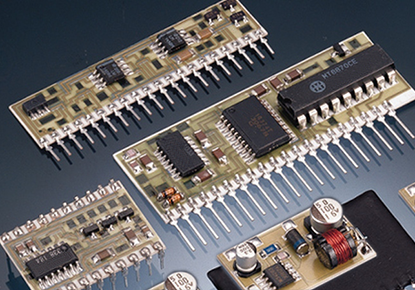
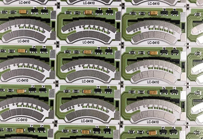
Manufacturing Process of Hybrid Integrated Circuits : |
The manufacturing process of Hybrid Integrated Circuits (HICs) involves similar steps to those of thin-film HICs, but with a few key differences due to the thicker nature of the film. Here is a general overview of the manufacturing process for thick-film HICs: 1, Substrate Preparation: The first step involves preparing the substrate, which can be made of materials such as alumina, aluminum nitride, or beryllium oxide. The substrate is cleaned and treated to ensure a clean surface for subsequent processes. 2, Thick-Film Printing: A thick film of conductive material, such as silver, gold, or palladium, is printed on the substrate using techniques such as screen printing, stenciling, or spraying. The thick film may also contain resistors and other passive components like capacitors, inductors, and thermistors, which are also patterned on the film through the same printing techniques. |
|
 |
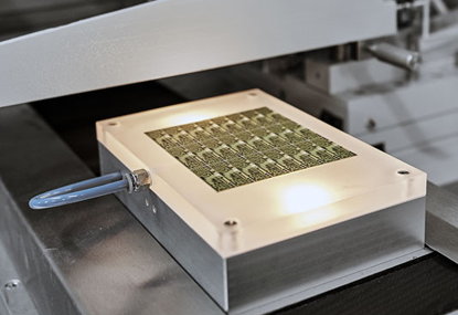
3, Drying and Firing: After printing and patterning, the Hybrid Integrated Circuit is dried and fired in a furnace to remove any solvents and binders and to sinter the conductive material. The firing process typically involves heating the circuit to high temperatures, typically around 700-900°C, for several minutes to achieve the desired properties. 4, Component Assembly: After the thick film is fired, discrete components, such as diodes, transistors, and integrated circuits, are attached to the substrate using epoxy or solder die attachment. The component placement must be precise to align with the circuit pattern defined on the thick film. 5, Wire Bonding: Wire bonding is used to establish electrical connections between the component leads and the circuit traces or pads on the substrate. The wire bonding process for thick-film Hybrid Integrated Circuit is similar to that of thin-film HICs and employs techniques such as ultrasonic or thermosonic bonding to bond thin wires made of materials like gold or aluminum. |
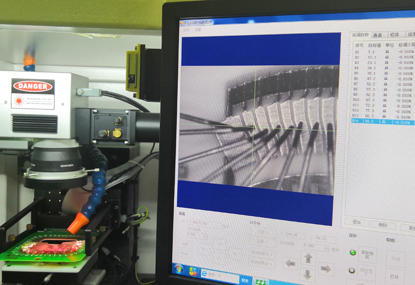
6, Encapsulation: Once the components are attached and wire bonded, the Hybrid Integrated Circuit is encapsulated to protect it from environmental factors. Encapsulation materials, such as epoxy or silicone, are applied to cover the components and wires. The encapsulation can take the form of molded packages or glob tops, providing mechanical protection and insulation. 7, Final Testing: Rigorous testing is performed to ensure the functionality, performance, and reliability of the manufactured Hybrid Integrated Circuits. Electrical tests, such as continuity checks, resistance measurements, and functional testing, are carried out to verify that the circuits meet the required specifications. Visual inspection and automated optical inspection (AOI) may be conducted to detect any manufacturing defects. |
|
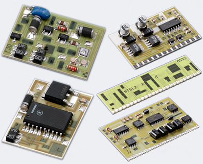
Applications of Hybrid Circuits : |
Hybrid Circuits combine the advantages of both integrated circuits (ICs) and discrete components, offering unique capabilities and enabling specific applications. Some common applications of hybrid integrated circuits include: 1, Automotive Electronics: Hybrid circuits play a significant role in automotive electronics, particularly in control modules, engine management systems, safety systems, and infotainment systems. They provide reliable performance, compact form factors, and integration of various functions in limited space. |
|
 |
2, Power Electronics: Hybrid integrated circuits are used in power electronic applications such as voltage regulators, motor drives, and power supplies. The integration of power semiconductors, gate drive circuits, and control logic within a single package improves system efficiency and reduces size and cost. 3, Aerospace and Defense: Hybrid circuits are widely used in aerospace and defense applications, where they provide high reliability, ruggedness, and ability to withstand harsh environments. They are used in radar systems, avionics, communication systems, electronic warfare systems, and missile guidance systems. 4, Industrial Control Systems: Hybrid integrated circuits are employed in industrial automation and control systems for tasks such as motor control, power management, sensor interfaces, and data acquisition. Their ability to integrate different functions into a single package helps in achieving compact and efficient control systems. |
5, Sensor and Measurement Systems: Hybrid circuits are beneficial in sensor and measurement systems where precise analog signal conditioning is required. They can integrate amplifiers, filters, and signal processing circuits with sensors to provide accurate measurements. 6, Telecommunications: Hybrid circuits are utilized in telecommunications equipment including base stations, repeaters, and transceivers. Their compact size and high-performance capabilities make them suitable for communication systems requiring efficient signal processing and transmission. 7, IoT and Wearable Devices: The compact size and integration capabilities of hybrid integrated circuits make them suitable for IoT devices and wearable electronics. They can combine sensors, microcontrollers, wireless communication modules, and power management circuits into a small form factor, enabling smart and connected devices. 8, Medical Devices: Hybrid circuits find application in medical devices such as implantable pacemakers, defibrillators, hearing aids, and monitoring systems. These circuits integrate active components like amplifiers and filters with passive components to achieve miniaturization and improved functionality in medical devices. |
|
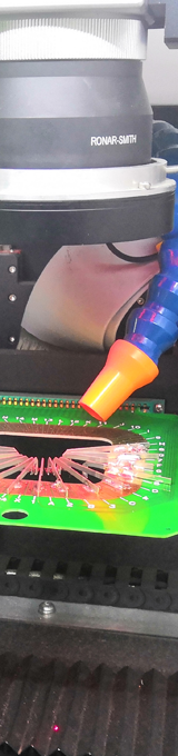
Laser Trimming Process of Hybrid Integrated Circuits : |
The laser trimming process is a critical step in the manufacturing of hybrid integrated circuits (ICs) to achieve precise and accurate electrical component values. Laser trimming is commonly used to adjust the resistance, capacitance, or other electrical parameters of thin film or thick film resistors and capacitors within the hybrid IC. The laser trimming process involves the following steps: 1, Precise Marking: The circuit components that require adjustment are marked with precision using techniques like photolithography or laser marking. This ensures that only the desired components are targeted during the trimming process. |
|
 |
2, Laser Ablation: A high-power laser beam is directed onto the marked areas of the circuit. The laser ablates or vaporizes the thin film or thick film material, effectively removing it from the circuit. The laser energy is carefully controlled to ensure precise removal of material according to the desired electrical adjustment. 3, Real-Time Monitoring: During the laser trimming process, real-time monitoring techniques, such as optical sensors or electrical measurements, are used to monitor the changes in electrical parameters. This allows for immediate feedback on the trimming progress and ensures that the desired values are achieved. 4, Iterative Trimming: The laser trimming process is typically an iterative process. After each round of laser ablation, the circuit is tested to measure the electrical parameters. If the desired values have not yet been achieved, the process is repeated until the targeted specifications are met. |
5, Quality Control: Once the desired electrical parameters are attained, the trimmed circuits undergo rigorous quality control testing to ensure their reliability and performance. This includes electrical testing, visual inspection, and any other required validation procedures. The laser trimming process offers several advantages for hybrid IC production. It enables precise and localized adjustments to electrical parameters, allowing for tighter tolerances and improved circuit performance. Laser trimming also offers non-contact processing, minimizing the risk of damage to delicate circuit components or surrounding materials. |
|
Monolithic VS Hybrid Integrated Circuits : |
Monolithic Integrated Circuits (MICs) and Hybrid Integrated Circuits (HICs) are two different approaches to electronic circuit integration. Here's a comparison between them for your reference: |
|
1, Monolithic Integrated Circuits: |
|
 |
1, Fabrication: Monolithic ICs are fabricated on a single semiconductor substrate, typically made of silicon. The entire circuit, including transistors, resistors, capacitors, and interconnects, is created on this substrate using various semiconductor processes such as diffusion, ion implantation, and deposition. 2, Integration Level: Monolithic ICs offer a high level of integration, enabling complex circuits to be integrated onto a single chip. This results in smaller size, lower power consumption, and improved performance compared to discrete components or hybrid circuits. 3, Cost: Once the fabrication process is established, monolithic IC production can be highly automated, leading to lower manufacturing costs per unit. However, the initial setup costs for designing and fabricating a monolithic IC can be high. |
4, Applications: Monolithic ICs are widely used in various electronic devices, including microprocessors, memory chips, and digital signal processors. They are suitable for applications where miniaturization, high performance, and cost-effectiveness are essential. |
|
2, Hybrid Integrated Circuits: |
|
 |
1, Fabrication: Hybrid Integrated Circuits combine multiple technologies, such as semiconductor chips, passive components, and thick film or thin film processes, into a single package. The components are individually manufactured and then interconnected using wire bonding, flip-chip, or other techniques. The interconnections are often made on a ceramic or organic substrate. 2, Integration Level: Hybrid Integrated Circuits offer a moderate level of integration, combining the advantages of different technologies. They can integrate both active (semiconductor) and passive (resistors, capacitors) components in a single package. This allows for higher power handling capabilities and flexibility in circuit design. 3, Flexibility: Hybrid ICs provide greater flexibility in terms of circuit design and customization. Different components from various manufacturers can be combined to meet specific requirements, making them suitable for applications with specialized needs. |
4, Applications: Hybrid Integrated Circuits are commonly used in aerospace, military, and high-reliability applications where robustness, high power handling, and the ability to withstand extreme operating conditions are crucial. They are also used in certain specialized applications, such as sensor interfaces and analog signal processing. Monolithic ICs offer higher integration levels, smaller size, and lower cost per unit, while hybrid ICs provide flexibility, higher power handling, and suitability for specialized applications. The choice between monolithic and hybrid integration depends on factors such as the desired level of integration, performance requirements, cost considerations, and the specific application's needs. |
|
Why PANDA PCB For Hybrid Circuits ? |
When it comes to the manufacturing and production of Hybrid Circuits, PANDA PCB Group stands out as a top choice. We provided superior circuit density, performances, and reliability, with relatively low development and tooling costs. We have over 20 years of experience in the design and manufacture of thick-film hybrid circuit products for high-reliability application in the industrial, medical, and military markets. |
|
 |
1, Expertise and Experience: PANDA PCB boasts a team of highly skilled engineers and technicians with extensive expertise in the field of hybrid circuits manufacturing. With years of experience, We possess in-depth knowledge and understanding of the complex processes involved in hybrid integration technology. 2, Advanced Manufacturing Facilities: Our Company is equipped with state-of-the-art manufacturing facilities that are specifically designed for producing high-quality hybrid circuits. We invests in the latest equipment, machinery, and tools, ensuring precision and efficiency throughout the production process. 3, Quality Assurance: Quality is a top priority at PANDA PCB. We follow stringent quality control measures at every stage of production to ensure that the hybrid circuits meet the highest standards. From material selection to final testing, We adhere to rigorous quality inspection procedures, resulting in reliable and durable hybrid integrated circuits. |
4, Cost-effectiveness: We offers competitive pricing without compromising on quality. We optimize their manufacturing processes to minimize production costs, allowing them to provide cost-effective solutions for hybrid integrated circuits. 5, Customization Capabilities: PANDA PCB understands that different applications may have unique requirements. We offer tailor-made solutions to meet specific customer needs. Whether it's the design, layout, or functionality, PANDA PCB works closely with clients to deliver customized HICs that perfectly match their application requirements. |
|
Design Guidelines of Thick Film Technology : |
Hybrid Integrated Circuit is manufactured based on Thick Film Technology, We compiled a Thick Film Technology-Design Guidelines as attached for you to download, It is to better support our customers' needs in designing and applying Hybrid Integrated Circuits, This guide covers detailed information on product solutions, engineering design specifications, material properties, available manufacturing processes, and more. We hope that this guide will assist customers in standardizing their design process while ensuring the manufacturability of the design data, ultimately improving product reliability and production efficiency. Customers are encouraged to refer to the guide when designing Thick Film Technologies to ensure adherence to best practices. |
Capabilities of Hybrid Integrated Circuits : |
1, Optional Processes of Hybrid Integrated Circuits :
Metalization Types : |
Thick Film Substrates (Screen-Printed) |
Thin Film Substrates (Photo-Imaged) |
|||
Process Types : |
TFM Capabilities |
HTCC / LTCC Capabilities |
DBC Capabilities |
DPC Capabilities |
AMB Capabilities |
Layer Counts : |
1, 2, 3, 4, 5, 6 Layers |
1, 2, 4, 6, 8, 10, 12 Layers |
1, 2 Layers |
1, 2 Layers |
1, 2 Layers |
Max Board Dimension : |
200*230mm |
200*200mm |
138*178mm |
138*190mm |
114*114mm |
Min Board Thickness : |
0.25mm |
0.25mm |
0.30mm~0.40mm |
0.25mm |
0.25mm |
Max Board Thickness : |
2.2mm |
2.0mm |
1L: 1.6mm; 2L 2.0mm |
2.0mm |
1.8mm |
Conductor Thickness : |
10um - 20um |
5um - 1500um |
1oz - 9oz |
1um - 1000um |
1oz- 22oz |
Min Line Width/Space : |
8/8mil (0.20/0.20mm) |
6/6mil (0.15/0.15mm) |
10/10mil (0.25/0.25mm) |
6/6mil (0.15/0.15mm) |
12/12mil (0.30/0.30mm) |
Substrates Types : |
AI203, ALN, BeO, ZrO2 |
AI203, ALN, BeO, ZrO2 |
Al2O3, AlN, ZrO2, PbO, SiO2, ZTA, Si3N4, SiC, Sapphire, Polycrystalline Silicon, Piezoelectric Ceramics |
Al2O3, AlN, ZrO2, PbO, SiO2, ZTA, Si3N4, SiC, Sapphire, Polycrystalline Silicon, Piezoelectric Ceramics |
AI203, ALN, BeO, ZrO2, Si3N4 |
Min Hole Diameter : |
4mil (0.15mm) |
4mil (0.15mm) |
4mil (0.1mm) |
4mil (0.1mm) |
4mil (0.1mm) |
Outline Tolerance : |
Laser: +/-0.05mm; Die Punch: +/-0.10mm |
Laser: +/-0.05mm; Die Punch: +/-0.10mm |
Laser: +/-0.05mm; Die Punch: +/-0.10mm |
Laser: +/-0.05mm; Die Punch: +/-0.10mm |
Laser: +/-0.05mm; Die Punch: +/-0.10mm |
Substrate Thickness : |
0.25, 0.38, 0.50, 0.635, 0.80,1.0, 1.25, 1.5, 2.0mm, Customizable |
0.25, 0.38, 0.50, 0.635, 0.80,1.0, 1.25, 1.5, 2.0mm, Customizable |
0.25, 0.38, 0.50, 0.635, 0.80,1.0, 1.25, 1.5, 2.0mm, Customizable |
0.25, 0.38, 0.50, 0.635, 0.80,1.0, 1.25, 1.5, 2.0mm, Customizable |
0.25, 0.38, 0.50, 0.635, 0.80,1.0, 1.25, 1.5, 2.0mm, Customizable |
Thickness Tolerance : |
0.25-0.38: +/-0.03mm; 0.50-2.00: +/-0.05mm |
0.25-0.38: +/-0.03mm; 0.50-2.00: +/-0.05mm |
0.25-0.38: +/-0.03mm; 0.50-2.00: +/-0.05mm |
0.25-0.38: +/-0.03mm; 0.50-2.00: +/-0.05mm |
0.25-0.38: +/-0.03mm; 0.50-2.00: +/-0.05mm |
Surface Treatment : |
Ag, Au, AgPd, AuPd |
Ag, Au, AgPd, AuPd, Mn/Ni |
OSP/Ni Plating, ENIG |
OSP/ENIG/ENEPIG |
OSP/ENIG/ENEPIG |
Min Solder PAD Dia : |
10mil (0.25mm) |
10mil (0.25mm) |
8mil (0.20mm) |
6mil (0.15mm) |
8mil (0.20mm) |
2, Optional Substrates of Hybrid Integrated Circuits :
Substrates : |
Alumina (Al2O3) |
Aluminum Nitride (AlN) |
Beryllium Oxide (BeO) |
Zirconium Dioxide (ZrO2) |
Max Application Temperature : |
662 - 1832 |
1832 |
2300 |
2432 |
Max Power Density (W/in²): |
75 |
1010 |
250 |
300 |
Max Ramp Up Speed (°F/sec): |
122 |
572 |
400 |
350 |
Thermal Conductivity (W/mK): |
20-35 |
180-220 |
200-300 |
2.0-5.0 |
Density (g/cm³): |
3.75 |
3.26 |
2.8 |
5.9 |
Dielectric Loss: |
0.0001 - 0.001 |
0.0001 - 0.0005 |
0.0001 - 0.0002 |
0.0005 - 0.001 |
Dielectric Constant: |
9.4 - 10.2 |
8.5 - 9.0 |
6.0 - 7.0 |
25 - 30 |
CTE, ppm/ºC: |
6.0 - 8.0 |
4.0 - 5.0 |
7.0 - 9.0 |
10.0 - 11.0 |
Substrate Thickness (mm): |
0.25 - 2.0 |
0.25 - 2.0 |
0.25 - 2.0 |
0.25 - 2.0 |
Typical Max. Dimension (inch): |
6 x 12 |
5 x 11 |
6 x 6 |
4 x 4 |
Theoretical Total Wattage (W): |
5400 |
55000 |
15000 |
20000 |
3, Conductive Paste of Hybrid Integrated Circuits :
Paste ( Materials) : |
Conductor Width/Space |
Soldering / Bonding |
Gold : |
8/8mil (0.20/0.20mm) |
Gold is a good conductor material and allows thermo-compression gold wire bonding and eutectic die attachment. It is, of course, costly and has poor solderability. |
Silver : |
8/8mil (0.20/0.20mm) |
Soldering & Silver is lower in cost, and solderable, but is not leach-resistant with tin/lead solders.More seriously, silver atoms migrate under the influence of DC electric fields, both causing short-circuits and reacting with many of the resistor paste formulations. |
Platinum-Silver : |
6/6mil (0.15/0.15mm) |
Soldering & Surface Mount, Palladium and platinum alloyed to the gold and silver produce good conductor pastes,with good adhesion to the substrate, good solderability, and moderately good wire bonding characteristics.. Copper and nickel are examples of materials that have been proposed for paste systems as substitutes for noble metals. |
Palladium-Silver : |
8/8mil (0.20/0.20mm) |
Soldering & Surface Mount ,Solderable, Wire bondable, (good aged adhesion general purpose), Silver-palladium conductor inks are the most commonly used materials, with both price and performance (primarily resistance to solder) increasing with palladium content. |
Platinum-Gold : |
6/6mil (0.15/0.15mm) |
Soldering & Au or Al Wire Bonding, Solderable (excellent aged adhesion with no migration). |
Palladium-Gold : |
8/8mil (0.20/0.20mm) |
Soldering & Au or Al Wire Bonding, Wire bondable. |
4, Resistive Paste of Hybrid Integrated Circuits :
Performances : |
Common Values/Range |
Description |
Resistance Value : |
1Ω to several MΩ |
The resistance value depends on the type and ratio of carbon black, typically ranging from 1Ω to Mega ohm. |
Resistance Tolerance : |
±1% to ±10% |
High-precision resistors can achieve ±0.1% tolerance used laser trimming process. |
Temperature Coefficient (TCR) : |
±50ppm/°C to ±200ppm/°C |
High-quality resistive paste should have a low TCR, preferably below ±100ppm/°C. |
Stability : |
≤1% |
Resistors must undergo high-temperature aging and humidity tests to ensure stability. |
Sintering Temperature : |
850°C to 950°C |
The sintering temperature for carbon paste depends on material properties, typically in this range. |
Conductivity : |
10⁶ S/m to 10⁸ S/m |
Conductivity depends on the type and ratio of carbon black, affecting resistance precision and stability. |
Surface Smoothness : |
Ra≤ 1 μm |
The surface must be free of cracks, bubbles, and non-uniform layers to ensure good mechanical and electrical properties. |
Insulation Resistance : |
≥10⁹ Ω |
Carbon paste should have good insulation properties to avoid leakage or short circuits. |
Mechanical Strength : |
≥100 MPa |
The resistive layer must have good compressive and bending strength to ensure the reliability of the resistor. |
Volatility : |
Solvent residue ≤ 1% |
High volatility solvents help with even coating and drying, but excessive volatility may affect electrical performance. |
Oxidation Resistance : |
>1000 hours |
High-quality carbon paste should have strong oxidation resistance to extend the service life. |
Humidity Resistance : |
≥1000 hours |
Resistors should be able to withstand high-humidity conditions to ensure long-term stable performance, no significant changes. |
5, Dielectric Paste of Hybrid Integrated Circuits :
1, High dielectric strength, That can be printed between two conductor layers as a insulating layer for Multilayer Thick Film Substrates. |
6, Insulating Layer of Hybrid Integrated Circuits :
The insulating layer is a critical component of hybrid integrated circuits (ICs), serving to electrically isolate various circuit elements and provide mechanical support for the components. The choice of insulating layer material depends on the specific application requirements and manufacturing process used. In hybrid ICs, the insulating layer typically serves as a substrate for the printing of thin film or thick film components such as resistors, capacitors, and interconnects. Common materials used as insulating layers in hybrid microcircuits include glass, thick-film polymer, and organic materials like epoxy or polyimide. 1, Glass-Glaze (Overglazes) is another insulating material that can be used in hybrid ICs. Glass substrates can be used as a base for thick-film resistors and other passive components, which are then applied using screen printing and firing techniques. Glass has good electrical and thermal properties but is more brittle than ceramic. 2, Thick-Film Polymer-based insulating materials can also be used in hybrid ICs. This involves applying a thick-film polymer material to a substrate, followed by curing at high temperatures to produce a hard, durable layer. Polymer insulating materials have the advantage of being flexible and less brittle than ceramics or glass. 3, Organic insulating materials, such as epoxy or polyimide, can be used in hybrid ICs. These materials offer good insulation properties, as well as flexibility and ease of use. Organic materials can be applied using photolithography or screen printing techniques, depending on the application. |