Thick Film Alumina PCB
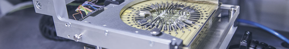
Thick Film Alumina PCBs are high-performance, high-reliability specialized circuit boards that utilize thick film technology to print conductive or resistive paste onto the surface of alumina substrates, which are then sintered at high temperatures to form stable circuit structures, offering excellent thermal conductivity, high-temperature resistance, and a low coefficient of thermal expansion, making them ideal choices for high-load or high-power electronic devices due to their outstanding reliability. Thick Film Alumina PCBs feature excellent thermal conductivity, effective heat dissipation, and superior electrical insulation. The thick-film technology provides strong and durable conductive traces, capable of handling high current loads. They also have low thermal expansion and excellent shock resistance, ensuring stable performance in harsh conditions like high temperatures and humidity. Thick Film Alumina PCBs are widely used in power modules, LED lighting, automotive electronics, aerospace, and industrial equipment. Their thermal conductivity and mechanical strength meet the demands of heat management and power transmission, ensuring reliability in high-temperature environments. As technology advances, their applications continue to expand, becoming key components in high-end electronics with high temperature, current, and load requirements. Fabrication Process of Thick Film Alumina PCB : |
 |
|
 |
1, Substrate Preparation: The first step in the process is to prepare the alumina ceramic substrate. The substrate is cleaned and polished to remove any impurities and to ensure a smooth surface. 2, Conductive or Resistive Paste Preparation: The conductive paste is prepared by mixing metal powders such as silver, gold, or copper with glass frit and organic binders. This paste is then screen printed onto the substrate using a stencil, to create the desired circuit pattern. 3, Drying: The printed substrate is then sent through a drying oven to remove any solvents used in the paste preparation process. This ensures that the paste is uniformly distributed on the substrate and ready for firing. |
|
4, Firing: The printed substrate is fired in a high-temperature furnace to fuse the conductive paste onto the substrate. The temperature and duration of the firing process depend on the paste composition, substrate material, and thickness. 5, Post-Firing: After firing, the substrate is allowed to cool before undergoing post-processing steps such as trimming the edges, drilling holes, applying solder mask, and surface finishing. 6, Testing: The final step in the process is to test the PCB for electrical continuity and functionality. This includes testing for short circuits, open circuits, and other defects that may affect the performance of the board. These fabrication processes are critical to ensuring the quality and reliability of thick film alumina PCBs, which are commonly used in high-power and high-reliability electronic applications. Please refer to Thick Film Resistor PCB for more informations. |
||
Advantages of Thick Film Alumina PCB : |
1, High Thermal Conductivity and High Temperature Applications: When electronics operate at elevated temperatures the materials used can have a substantial impact on performance and life. With its ability to dispel heat, ceramic substrate performs better and can prevent a device from being damaged by high temperatures. Depending on the material used, like Alumina or Aluminum Oxide, Aluminum nitride (AlN), beryllia or beryllium oxide (BeO), silicon carbide (SiC), and boron nitride (BN), the values range from 20 to 300 W/(m·K). It is way beyond that of FR-4 printe circuit board, more than 20x higher. 2, Low Coefficient of Thermal Expansion (CTE): Thick film alumina PCBs has solid and outstanding interatomic bonds, so Ceramic hybrid circuits can withstand high temperatures and is still firm, stable, and steady even under changing temperatures. |
|
 |
3, Low Failure Rate: Aside from long term reliability, Thick film alumina PCBs also exhibit a lower mean time between failure rate when exposed to environmental stresses such as high temperature, mechanical vibration or other harsh conditions. 4, Multi-Layering: A multi-layer hybrid circuit can do a more complicated task. With the toughness of its material, another layer can be added easily and still keep the other components safe. Thick film alumina PCB is excellent for heavy-duty applications. 5, Excellent Thermal Insulation: Thick film alumina PCBs is incredibly insulating; therefore, heat will be less likely to flow through the substrate, preserving the ceramic hybrid circuit's components from getting damaged or harmed. 6, Small Size and Weight: In applications where a high premium is placed on small size and weight, such as aircraft, missiles, Thick film alumina PCBs can offer an extremely compact, high performance solution. 7, Long Term Reliability: Most commercially packaged semiconductors will have a life span measured in years, while alumina PCBs have a life span measured in decades. |
8, High Frequency: High frequency can be handled by a hybrid circuit with its dimensional and thermal stability. Industries requiring high-frequency data and electrical signal transmissions. 9, Wide Range of Applications: Thick film alumina PCBs are used in a variety of high-power applications such as power modules, LED lighting, automotive electronics, and industrial equipment. 10, Cost-Effective: Thick film alumina PCBs are more cost-effective compared to other high-temperature substrates such as ceramic printed circuit boards (PCBs). 11, Precise Patterning: The thick film conductive layer on the alumina substrate allows for precise patterning of circuit traces, pads, and components such as resistors and capacitors. 12, Customizable: Thick film alumina PCBs can be customized to meet specific application requirements, including substrate thickness, conductive paste composition, and surface finish. |
|
Design Guideline of Thick Film Alumina PCB : |
 |
1, Ceramic Substrates: In addition to 96% or 98% Alumina (Al2O3) and Beryllium Oxide (BeO), other ceramic substrate materials such as aluminum nitride (AlN) and silicon carbide (SiC) are also available. The thickness range may vary depending on the manufacturer. 2, Conductive Paste Materials: Other conductive paste materials such as copper, nickel, and platinum are also available. The choice of material depends on the application requirements and cost considerations. 3, Thickness of The Conductors: The thickness of the conductors can range from a few microns to several tens of microns, such as 12um+/-5um, depending on the specific application requirements. 4, Minimum Trace Width and Space: The minimum trace width and space may vary depending on the manufacturer's capabilities and equipment. Some manufacturers can produce traces as small as 0.2mm/0.15mm in volume production. 5, Resistor Value Tolerance: The resistor value tolerance can be customized to meet specific application requirements. Laser trimming can achieve higher precision and tighter tolerances. |
6, Gold and Silver Palladium: While both gold and silver palladium are workable for gold-wire bonding, special silver palladium is recommended for applications that require high reliability and long-term stability. 7, Gold-Palladium: Gold-palladium is indeed more expensive than silver due to the higher cost of gold as a material. 8, More Different Resistor Values: The number of different resistor values designed onto the board may affect the cost of the board, but it ultimately depends on the manufacturer's pricing policies and production capabilities. |
|
Typical Applications of Thick Film Alumina PCB : |
Thick Film Alumina PCBs are utilized in a wide range of high-power and high-reliability applications due to their excellent thermal conductivity, electrical insulation, and mechanical robustness. Some typical applications include: 1, Power Electronics: Thick Film Alumina PCBs are commonly used in power electronic modules such as inverters, motor drives, and power supplies due to their ability to efficiently dissipate heat and provide electrical insulation. 2, LED Lighting: Thick Film Alumina PCBs are well-suited for LED lighting applications where thermal management is critical. They help in maintaining the operational efficiency and longevity of LED fixtures. |
 |
3, Automotive Electronics: In the automotive industry, Thick Film Alumina PCBs find applications in power control units, engine control modules, and other electronic systems that require reliable performance in high-temperature environments. 4, Industrial Equipment: Various industrial equipment such as heavy-duty machinery, process control systems, and power distribution units utilize Thick Film Alumina PCBs for their durability and reliability in demanding operating conditions. |
|
5, Renewable Energy Systems: Thick Film Alumina PCBs are employed in solar inverters, wind turbine converters, and other renewable energy systems where efficient heat dissipation and high electrical insulation are essential. 6, Aerospace and Defense: In aerospace and defense applications, Thick Film Alumina PCBs are utilized in radar systems, avionics, communication equipment, and power management units due to their ability to withstand harsh environmental conditions and temperature variations. 7, Medical Devices: Thick Film Alumina PCBs are used in medical devices and equipment where reliability, thermal management, and electrical insulation are crucial for safe and consistent operation. |
 |
8, Telecommunications: They are also used in telecommunications infrastructure, including base stations, signal processing equipment, and power amplifiers, to ensure reliable performance in high-frequency and high-power applications. These applications demonstrate the versatility and reliability of Thick Film Alumina PCBs in various industries where high-performance electronic systems are required. |
|
Automotive Applications of Thick Film Alumina PCB : |
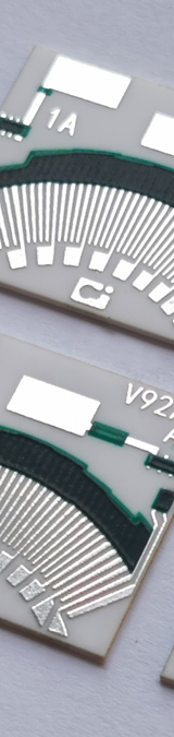
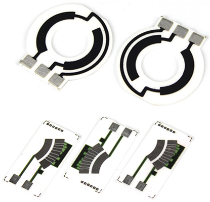
1, Fuel Level Sensor PCB: These sensors are used to measure the amount of fuel in a vehicle's tank. Thick Film Alumina PCBs provide an excellent substrate for fuel level sensors due to their high thermal conductivity and electrical insulation properties. They can withstand the harsh conditions inside the fuel tank while accurately measuring the fuel level. The Thick Film Alumina PCBs in fuel level sensors offer several advantages: ● Resistance to temperature variations and chemical exposure, ensuring reliable performance in harsh automotive environments. ● High precision and accuracy in fuel level measurement, enabling accurate reading of remaining fuel quantity. ● Compact size and lightweight design, allowing easy integration into the fuel system. |
|
 |
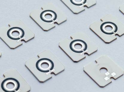
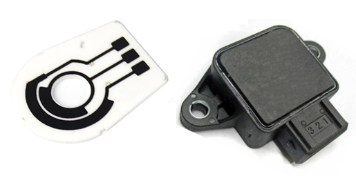
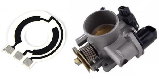
2, Throttle Position Sensor PCB: Throttle position sensors are responsible for detecting the position of the throttle valve in the engine's intake system. This information is crucial for determining the engine load and adjusting fuel injection accordingly. Thick film alumina PCBs are well-suited for these sensors as they offer good mechanical stability and resistance to temperature variations. Key benefits of using thick film alumina PCBs in throttle position sensors include: ● Excellent thermal stability, ensuring consistent performance across a wide range of temperatures. ● High mechanical strength, allowing the sensor to withstand vibrations and shocks associated with automotive applications. ● Compatibility with high-power circuits, enabling accurate measurement and transmission of throttle position data. ● Enhanced electrical insulation properties, ensuring safe and reliable operation. |
Thick Film Alumina PCBs provide a reliable substrate for the sensors, ensuring accurate measurement and long-term performance. Their high electrical insulation capability helps maintain signal integrity, while their ability to withstand high temperatures makes them suitable for use in the demanding automotive environment. It's worth noting that Thick Film Alumina PCBs can have other applications in the automotive industry beyond these examples. They are often utilized in various sensor and control systems, such as oxygen sensors, engine control units (ECUs), transmission control modules (TCMs), and ABS brake systems, as mentioned in the previous response. |
|
Typical Capabilities of Thick Film Alumina PCB : |
1, Optional Processes of Thick Film Alumina PCB :
Metalization Types : |
Thick Film Substrates (Screen-Printed) |
Thin Film Substrates (Photo-Imaged) |
|||
Process Types : |
TFM Capabilities |
HTCC / LTCC Capabilities |
DBC Capabilities |
DPC Capabilities |
AMB Capabilities |
Layer Counts : |
1, 2, 3, 4, 5, 6 Layers |
1, 2, 4, 6, 8, 10, 12 Layers |
1, 2 Layers |
1, 2 Layers |
1, 2 Layers |
Max Board Dimension : |
200*230mm |
200*200mm |
138*178mm |
138*190mm |
114*114mm |
Min Board Thickness : |
0.25mm |
0.25mm |
0.30mm~0.40mm |
0.25mm |
0.25mm |
Max Board Thickness : |
2.2mm |
2.0mm |
1L: 1.6mm; 2L 2.0mm |
2.0mm |
1.8mm |
Conductor Thickness : |
10um - 20um |
5um - 1500um |
1oz - 9oz |
1um - 1000um |
1oz- 22oz |
Min Line Width/Space : |
8/8mil (0.20/0.20mm) |
6/6mil (0.15/0.15mm) |
10/10mil (0.25/0.25mm) |
6/6mil (0.15/0.15mm) |
12/12mil (0.30/0.30mm) |
Substrates Types : |
AI203, ALN, BeO, ZrO2 |
AI203, ALN, BeO, ZrO2 |
Al2O3, AlN, ZrO2, PbO, SiO2, ZTA, Si3N4, SiC, Sapphire, Polycrystalline Silicon, Piezoelectric Ceramics |
Al2O3, AlN, ZrO2, PbO, SiO2, ZTA, Si3N4, SiC, Sapphire, Polycrystalline Silicon, Piezoelectric Ceramics |
AI203, ALN, BeO, ZrO2, Si3N4 |
Min Hole Diameter : |
4mil (0.15mm) |
4mil (0.15mm) |
4mil (0.1mm) |
4mil (0.1mm) |
4mil (0.1mm) |
Outline Tolerance : |
Laser: +/-0.05mm; Die Punch: +/-0.10mm |
Laser: +/-0.05mm; Die Punch: +/-0.10mm |
Laser: +/-0.05mm; Die Punch: +/-0.10mm |
Laser: +/-0.05mm; Die Punch: +/-0.10mm |
Laser: +/-0.05mm; Die Punch: +/-0.10mm |
Substrate Thickness : |
0.25, 0.38, 0.50, 0.635, 0.80,1.0, 1.25, 1.5, 2.0mm, Customizable |
0.25, 0.38, 0.50, 0.635, 0.80,1.0, 1.25, 1.5, 2.0mm, Customizable |
0.25, 0.38, 0.50, 0.635, 0.80,1.0, 1.25, 1.5, 2.0mm, Customizable |
0.25, 0.38, 0.50, 0.635, 0.80,1.0, 1.25, 1.5, 2.0mm, Customizable |
0.25, 0.38, 0.50, 0.635, 0.80,1.0, 1.25, 1.5, 2.0mm, Customizable |
Thickness Tolerance : |
0.25-0.38: +/-0.03mm; 0.50-2.00: +/-0.05mm |
0.25-0.38: +/-0.03mm; 0.50-2.00: +/-0.05mm |
0.25-0.38: +/-0.03mm; 0.50-2.00: +/-0.05mm |
0.25-0.38: +/-0.03mm; 0.50-2.00: +/-0.05mm |
0.25-0.38: +/-0.03mm; 0.50-2.00: +/-0.05mm |
Surface Treatment : |
Ag, Au, AgPd, AuPd |
Ag, Au, AgPd, AuPd, Mn/Ni |
OSP/Ni Plating, ENIG |
OSP/ENIG/ENEPIG |
OSP/ENIG/ENEPIG |
Min Solder PAD Dia : |
10mil (0.25mm) |
10mil (0.25mm) |
8mil (0.20mm) |
6mil (0.15mm) |
8mil (0.20mm) |
2, Optional Substrates of Thick Film Alumina PCB :
Substrates : |
Alumina (Al2O3) |
Aluminum Nitride (AlN) |
Beryllium Oxide (BeO) |
Zirconium Dioxide (ZrO2) |
Max Application Temperature : |
662 - 1832 |
1832 |
2300 |
2432 |
Max Power Density (W/in²): |
75 |
1010 |
250 |
300 |
Max Ramp Up Speed (°F/sec): |
122 |
572 |
400 |
350 |
Thermal Conductivity (W/mK): |
20-35 |
180-220 |
200-300 |
2.0-5.0 |
Density (g/cm³): |
3.75 |
3.26 |
2.8 |
5.9 |
Dielectric Loss: |
0.0001 - 0.001 |
0.0001 - 0.0005 |
0.0001 - 0.0002 |
0.0005 - 0.001 |
Dielectric Constant: |
9.4 - 10.2 |
8.5 - 9.0 |
6.0 - 7.0 |
25 - 30 |
CTE, ppm/ºC: |
6.0 - 8.0 |
4.0 - 5.0 |
7.0 - 9.0 |
10.0 - 11.0 |
Substrate Thickness (mm): |
0.25 - 2.0 |
0.25 - 2.0 |
0.25 - 2.0 |
0.25 - 2.0 |
Typical Max. Dimension (inch): |
6 x 12 |
5 x 11 |
6 x 6 |
4 x 4 |
Theoretical Total Wattage (W): |
5400 |
55000 |
15000 |
20000 |
3, Conductive Paste of Thick Film Alumina PCB :
Paste ( Materials) : |
Conductor Width/Space |
Soldering / Bonding |
Gold : |
8/8mil (0.20/0.20mm) |
Gold is a good conductor material and allows thermo-compression gold wire bonding and eutectic die attachment. It is, of course, costly and has poor solderability. |
Silver : |
8/8mil (0.20/0.20mm) |
Soldering & Silver is lower in cost, and solderable, but is not leach-resistant with tin/lead solders.More seriously, silver atoms migrate under the influence of DC electric fields, both causing short-circuits and reacting with many of the resistor paste formulations. |
Platinum-Silver : |
6/6mil (0.15/0.15mm) |
Soldering & Surface Mount, Palladium and platinum alloyed to the gold and silver produce good conductor pastes,with good adhesion to the substrate, good solderability, and moderately good wire bonding characteristics. Copper and nickel are examples of materials that have been proposed for paste systems as substitutes for noble metals. |
Palladium-Silver : |
8/8mil (0.20/0.20mm) |
Soldering & Surface Mount ,Solderable, Wire bondable, (good aged adhesion general purpose), Silver-palladium conductor inks are the most commonly used materials, with both price and performance (primarily resistance to solder) increasing with palladium content. |
Platinum-Gold : |
6/6mil (0.15/0.15mm) |
Soldering & Au or Al Wire Bonding, Solderable (excellent aged adhesion with no migration). |
Palladium-Gold : |
8/8mil (0.20/0.20mm) |
Soldering & Au or Al Wire Bonding, Wire bondable. |
4, Resistive Paste of Thick Film Alumina PCB :
Performances : |
Common Values/Range |
Description |
Resistance Value : |
1Ω to several MΩ |
The resistance value depends on the type and ratio of carbon black, typically ranging from 1Ω to Mega ohm. |
Resistance Tolerance : |
±1% to ±10% |
High-precision resistors can achieve ±0.1% tolerance used laser trimming process. |
Temperature Coefficient (TCR) : |
±50ppm/°C to ±200ppm/°C |
High-quality resistive paste should have a low TCR, preferably below ±100ppm/°C. |
Stability : |
≤1% |
Resistors must undergo high-temperature aging and humidity tests to ensure stability. |
Sintering Temperature : |
850°C to 950°C |
The sintering temperature for carbon paste depends on material properties, typically in this range. |
Conductivity : |
10⁶ S/m to 10⁸ S/m |
Conductivity depends on the type and ratio of carbon black, affecting resistance precision and stability. |
Surface Smoothness : |
Ra≤ 1 μm |
The surface must be free of cracks, bubbles, and non-uniform layers to ensure good mechanical and electrical properties. |
Insulation Resistance : |
≥10⁹ Ω |
Carbon paste should have good insulation properties to avoid leakage or short circuits. |
Mechanical Strength : |
≥100 MPa |
The resistive layer must have good compressive and bending strength to ensure the reliability of the resistor. |
Volatility : |
Solvent residue ≤ 1% |
High volatility solvents help with even coating and drying, but excessive volatility may affect electrical performance. |
Oxidation Resistance : |
>1000 hours |
High-quality carbon paste should have strong oxidation resistance to extend the service life. |
Humidity Resistance : |
≥1000 hours |
Resistors should be able to withstand high-humidity conditions to ensure long-term stable performance, no significant changes. |
5, Dielectric Paste of Thick Film Alumina PCB :
1, High dielectric strength: It possesses a high dielectric strength, enabling it to be printed between two conductor layers as an insulating layer for Multilayer-Thick Film Hybrid Circuits. This ensures proper insulation and prevents electrical shorts between the conductive layers. 2, Good insulation resistance: The dielectric paste exhibits excellent insulation resistance properties. It can be printed and applied as a protective layer on top of the conductor layer, further enhancing insulation and preventing leakage currents. 3, Low power factor: In certain applications, the dielectric paste can be printed on a metal core (e.g., stainless steel) to serve as an insulating layer for thick film heating elements. Its low power factor helps minimize energy losses and ensures efficient heat transfer. 4, High dielectric constant for resistor elements: When fabricating thick film resistor elements, having a high dielectric constant is advantageous. However, it is important to note that a dielectric constant of around 10 is typically the maximum achievable value, as materials with higher dielectric constants may exhibit thermal coefficient problems. Thus, a balance must be struck between dielectric constant and stability for applications requiring resistor element stability. The dielectric paste in Thick Film Alumina PCBs plays a critical role in providing insulation, preventing electrical shorts, and ensuring the reliable performance of various circuit elements. |