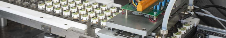
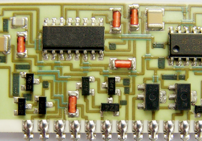
Thick Film Hybrid Integrated Circuits
Thick Film Hybrid Integrated Circuits are electronic components produced by combining thick film technology with hybrid integration processes, which involve steps like selecting ceramic substrates, using screen printing to apply conductive, dielectric, and resistive materials, high-temperature sintering for material adhesion, laser trimming for precise resistance adjustment, assembling components like chips and sensors, and final packaging and testing to ensure high reliability, performance, and suitability for demanding applications such as automotive electronics, aerospace, and military communications. Thick Film Hybrid Integrated Circuits offer unique features that make them suitable for a wide range of applications. They are designed using thick film technology, which enables the integration of both passive components (resistors, capacitors) and active components (transistors, diodes) onto the same ceramic substrate. This integration results in circuits that are compact and highly reliable, with improved performance in harsh environments. Thick Film Hybrid Integrated Circuits are widely used in automotive, telecommunications, medical, aerospace, and military equipment. In automotive electronics, they are found in engine control units, sensors, and other critical components. In telecommunications, they are used in signal processing and RF circuits. Their high-temperature and high-pressure stability make them vital in aerospace and military applications, where reliability is crucial. Features of Thick Film Hybrid Integrated Circuits : |
 |
|
 |
1. Low Power Consumption: Hybrid integrated circuits consume minimal power requiring minimal maintenance due to low heat generation. 2. Compact Size: Thick Film Hybrid integrated circuits are small, compact and lightweight making them easy to install in different devices. 3. Robustness: Hybrid technology can support rugged applications that require high levels of resilience and compatibility with other systems’ requirements. 4. Customizable Design: They can be designed to meet specific application needs with a customized combination of passive and active components. 5. Improved Signal-To-Noise Ratio: Hybrid integrated circuitry has better shielding from noise because of its sealed construction during production. |
|
6. Easy To Repair And Modify: Thick Film Hybrid integrated circuits can be easily repaired, replaced or modified through the stacked structure which allows for individual component replacement if need be. Thick Film Hybrid Integrated Circuit's mass production capability, reliability, and building-block approach to integrated circuit design have ensured the rapid adoption of standardized ICs in place of designs using discrete transistors. Please refer to Thick Film Technology for more informations. |
||
Printing Techniques in Thick Film Hybrid Integrated Circuits : |
Thick film printing techniques play a crucial role in Thick Film Hybrid Integrated Circuits by enabling the printing of various functional layers on a substrate to create electronic components. These techniques include screen printing, stencil printing, and inkjet printing, among others. |
|
 |
1, Material Printing: These techniques allow for precise printing of conductive, resistive, and dielectric materials onto the substrate, enabling the creation of circuit traces, resistors, and capacitors. 2, Customization and Flexibility: Thick film printing techniques provide the flexibility to customize circuit designs and patterns, making it easier to produce customized and specialized circuits for specific applications. 3, Miniaturization: With advancements in thick film printing techniques, it is possible to create miniaturized components, leading to higher component density and improved integration within the circuit. 4, Cost-Effectiveness: Compared to traditional thin film printing methods, thick film printing techniques are generally more cost-effective, making them suitable for large-scale production of integrated circuits. |
5, Reliability and Durability: Thick film printing techniques contribute to the creation of robust and reliable components, with good adhesion to the substrate and excellent thermal and mechanical properties. Thick film printing techniques are essential for fabricating Thick Film Hybrid Integrated Circuits, as they enable the precise printing of functional materials, customization, miniaturization, cost-effectiveness, and the creation of reliable electronic components. |
|
Advantages of Thick Film Hybrid Integrated Circuits : |
1, Wide Application Range: Thick Film Hybrid Integrated Circuits find application in diverse fields such as automotive electronics, telecommunications, aerospace, medical equipment, and industrial control systems. They can perform functions like signal conditioning, amplification, power management, and sensor interfacing. |
|
 |
2, Mixed Technology Integration: Thick Film Hybrid Integrated Circuits combine thick film technology with semiconductor integrated circuits, enabling the integration of both passive and active components on a single substrate. This integration enhances performance and functionality while reducing the need for external components. 3, Compact and Miniaturized: Thick Film Hybrid Integrated Circuits are known for their compact size and high component density. The integration of passive components into the circuit substrate allows for miniaturization, making them ideal for space-constrained applications. 4, High Reliability: Thick Film Hybrid Integrated Circuits are known for their robustness and reliability. The thick film materials exhibit excellent thermal stability, mechanical strength, and resistance to environmental factors such as moisture, humidity, and temperature variations. 5, Customization and Flexibility: Thick Film Hybrid Integrated Circuits offer flexibility in design and customization. Different types of resistors, capacitors, and conductors can be printed and tailored to specific requirements, allowing for optimized circuit performance and functionality. |
6, Cost-Effective: Thick Film Integrated Circuits based on Thick Film Technology are generally more cost-effective compared to other integration technologies. The use of screen printing techniques and ceramic substrates contributes to efficient manufacturing processes and lower production costs. 7, Enhanced Functionality: The integration of both passive and active components on a single substrate enables enhanced functionality and performance. This integration eliminates the need for external components, reducing circuit complexity and improving overall system efficiency. |
|
Applications of Thick Film Hybrid Integrated Circuits : |
Thick Film Hybrid Integrated Circuits find application in various fields due to their unique properties and advantages. Here are some common applications of Thick Film Integrated Circuits: 1, Automotive Electronics: Thick Film Hybrid Integrated Circuits are extensively utilized in automotive applications due to their ruggedness and reliability. They are used in engine control units, airbag control systems, anti-lock braking systems, and various other automotive electronic control modules. |
|
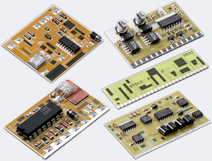 |
2, Sensors: Thick Film Hybrid Integrated Circuits are widely used in sensor applications, including temperature sensors, pressure sensors, humidity sensors, and gas sensors. The thick film technology allows for the integration of sensing elements and signal conditioning circuitry on a single chip, enabling efficient and compact sensor devices. 3, Power Electronics: Thick Film Hybrid Integrated Circuits play a crucial role in power electronics applications. They are utilized in power management circuits, voltage regulators, motor control circuits, and switch-mode power supplies. The ability to integrate passive components with active devices enables efficient power conversion and control. 4, Communication Systems: Thick Film Hybrid Integrated Circuits are employed in communication systems, including wireless transceivers, RF amplifiers, and frequency synthesizers. They enable the integration of RF (Radio Frequency) components, filters, and matching circuits in compact and cost-effective modules. |
5, Signal Conditioning: Thick Film Hybrid Integrated Circuits are employed in signal conditioning circuits, which are responsible for amplifying, filtering, and processing analog signals from sensors or other sources. They are commonly used in applications such as instrumentation, data acquisition systems, and industrial control systems. 6, Display Technology: Thick Film Integrated Circuits find application in display technologies, including LCD (Liquid Crystal Display) drivers and OLED (Organic Light-Emitting Diode) drivers. They provide the necessary driving signals to control the pixels and segments in displays, enabling the generation of images and information. |
|
Laser Trimming of Thick Film Hybrid Integrated Circuits : |
 |
● Laser Trimming of Thick Film Hybrid Integrated Circuits refers to the process of using laser technology to adjust or trim the resistors or other passive components on a thick film hybrid circuit. This trimming process is used to fine-tune the electrical characteristics of the circuit and achieve precise resistance values or component performance. Laser trimming offers high precision and allows for accurate adjustment without physically altering the circuit layout. It is commonly employed in the production of electronic devices that require precise and stable circuit performance. During laser trimming, resistors in hybrid circuits are adjusted to the exact resistance value. |
● During the trimming process, the respective output signal is constantly measured and compared with the nominal value, When the target value is reached, the laser cut is automatically stopped. The thick film resistor after laser trimming process can be controlled within +/-1%, or to be more tighter of +/-0.5%. |
|
Stack-Up of Thick Film Hybrid Integrated Circuits : |
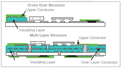 |
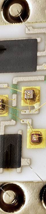
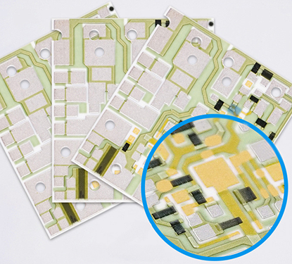
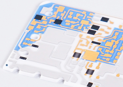
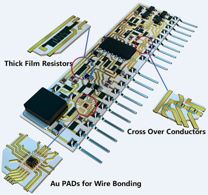
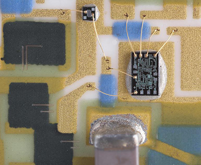
● Stack-Up of Thick Film Hybrid Integrated Circuits refers to the arrangement or layering of different materials in a hybrid circuit during its manufacturing process. This process involves the stacking and integration of multiple layers, including the substrate, ceramic or polyimide layers, conductor layers, resistor layer, and dielectric layers. The thick film hybrid circuits are constructed by printing a combination of conductive and resistive inks on ceramic substrates as the base layers. ● Thick Film Hybrid Integrated Circuits are a highly sophisticated technology for the production of wiring supports that has been in use for decades. The conductor tracks are applied by screen printing and then burned in. The use of ceramic as substrate enables highest reliability under the harshest environmental conditions. |
● The stack-up of these materials allows for the interconnection of the different components on the circuit, such as resistors, capacitors, and transistors, with the necessary wiring. The different layers of the stack-up can be designed to facilitate electrical signals to pass through specific areas of the circuit, which helps in determining the overall functionality and performance of the hybrid circuit. The stack-up design plays a critical role in achieving optimal performance, stable operation, and long-term reliability of thick film hybrid integrated circuits. |
|
Design Guideline of Thick Film Hybrid Integrated Circuits : |
Designing Thick Film Hybrid Integrated Circuits involves several important guidelines to ensure the successful development of the circuits. Here are some key points to consider: 1, Process Selection: Choose a suitable process flow for Thick Film Hybrid Integrated Circuits design, including both thick film and integrated circuit processes, to ensure the realization of the required device structure and performance. |
|
 |
2, Device Design: Design device structures that are compatible with the thick film process, including transistors, resistors, capacitors, and other components. Consider the specific characteristics of the thick film process and carefully plan device dimensions, layout, and interconnections. 3, Electrical Characteristics: Focus on the electrical characteristics of the devices during the design process, including voltage-current characteristics, frequency response, noise, etc., to ensure that the designed devices meet the performance requirements of the system. 4, Thermal Characteristics: Thick film hybrid integrated circuits generate heat during operation, so it is important to consider thermal coupling of devices and design effective heat dissipation solutions to ensure stable and reliable device operation. 5, Reliability: Consider the long-term reliability of the devices, including the impact of temperature variations, voltage fluctuations, electromagnetic interference, etc. Design appropriate protection and compensation measures for reliable performance over time. |
|
6, Cost and Manufacturing Process: Consider cost and manufacturing process factors during the design phase, select a rational design approach, and optimize it in consideration of actual production conditions to ensure the design can be effectively realized in manufacturing. |
|
Multilayer Printing of Thick Film Hybrid Integrated Circuits : |
The production process of multilayer printing technology used for Thick Film Hybrid Integrated Circuits involves several challenging aspects. 1, Alignment and Registration: Achieving accurate alignment and registration of multiple layers is crucial for ensuring proper functionality of the circuit. The precise alignment of different layers during printing can be challenging due to factors such as substrate warping, thermal expansion, and dimensional variations. 2, Film Patterning and Resolution: Creating intricate patterns and high-resolution features on each layer is a significant challenge in multilayer printing. Factors such as ink formulation, printing technique, and substrate surface quality can impact the achievable resolution and pattern fidelity. |
|
 |
3, Material Compatibility: Thick film hybrid integrated circuits often require the printing of multiple materials with different compositions and properties. Ensuring compatibility between these materials is essential to avoid issues such as delamination, interdiffusion, or chemical reactions that may affect device performance and reliability. 4, Layer Thickness Control: Controlling the thickness of each printed layer is critical to achieve the desired electrical and mechanical properties of the circuit. However, achieving uniform layer thickness across the substrate can be difficult due to variations in ink viscosity, printing pressure, and substrate surface irregularities. 5, Thermal Processing: Thick film printing techniques typically involve thermal processing steps, such as drying, firing, or sintering, to achieve optimal material properties. Managing the thermal profile during these processes is critical to prevent defects like cracks, voids, or excessive shrinkage that can compromise circuit integrity. |
6, Yield and Reproducibility: Maintaining consistent printing quality and achieving high yield rates are ongoing challenges in multilayer printing technology. Process variations, such as ink formulation, printing parameters, and curing conditions, can impact the reproducibility and yield of the fabricated circuits. Addressing these technical challenges requires continuous process optimization, advanced equipment, and stringent quality control measures. Overcoming these difficulties ensures the successful implementation of multilayer printing technology for Thick Film Hybrid Integrated Circuits, enabling the production of reliable and high-performance electronic components. |
|
Why PANDA PCB For Thick Film Hybrid Integrated Circuits ? |
At PANDA PCB Group, We specialize in designing and manufacturing Thick Film Hybrid Integrated Circuits for high-reliability applications in the industrial, medical, and military markets. With over 20 years of experience, our products offer superior circuit density, performance, and reliability, all while keeping development and tooling costs relatively low. Our comprehensive manufacturing solution covers everything from initial layout design to final testing and inspection. |
|
 |
● Our capabilities include the manufacturing of Thick Film Hybrid Integrated Circuits, soldered hybrids, through-hole metallizations in ceramics, bonding hybrids, and multilayer circuits (up to 4 conductor layers per side). This allows us to provide multilayer hybrid circuits up to 8 layers, utilizing screen-printing insulating dielectric to ensure connections between layers are made only where required, enhancing integration. The market for hybrid circuits is segmented into hermetic packaging and non-hermetic packaging based on packaging type. ● Furthermore, It is also segmented by end-use industries such as aerospace & defense, automotive, industrial, consumer electronics, healthcare, power generation, oil & gas, and others. Our thick film products are customized solutions tailored to meet the specific requirements of our customers. Through focused R&D projects in the field of microsystems, we are continuously developing Thick Film Technology for future advancements. |
Capabilities of Thick Film Hybrid Integrated Circuits : |
1, Optional Processes of Thick Film Hybrid Integrated Circuits :
Metalization Types : |
Thick Film Substrates (Screen-Printed) |
Thin Film Substrates (Photo-Imaged) |
|||
Process Types : |
TFM Capabilities |
HTCC / LTCC Capabilities |
DBC Capabilities |
DPC Capabilities |
AMB Capabilities |
Layer Counts : |
1, 2, 3, 4, 5, 6 Layers |
1, 2, 4, 6, 8, 10, 12 Layers |
1, 2 Layers |
1, 2 Layers |
1, 2 Layers |
Max Board Dimension : |
200*230mm |
200*200mm |
138*178mm |
138*190mm |
114*114mm |
Min Board Thickness : |
0.25mm |
0.25mm |
0.30mm~0.40mm |
0.25mm |
0.25mm |
Max Board Thickness : |
2.2mm |
2.0mm |
1L: 1.6mm; 2L 2.0mm |
2.0mm |
1.8mm |
Conductor Thickness : |
10um - 20um |
5um - 1500um |
1oz - 9oz |
1um - 1000um |
1oz- 22oz |
Min Line Width/Space : |
8/8mil (0.20/0.20mm) |
6/6mil (0.15/0.15mm) |
10/10mil (0.25/0.25mm) |
6/6mil (0.15/0.15mm) |
12/12mil (0.30/0.30mm) |
Substrates Types : |
AI203, ALN, BeO, ZrO2 |
AI203, ALN, BeO, ZrO2 |
Al2O3, AlN, ZrO2, PbO, SiO2, ZTA, Si3N4, SiC, Sapphire, Polycrystalline Silicon, Piezoelectric Ceramics |
Al2O3, AlN, ZrO2, PbO, SiO2, ZTA, Si3N4, SiC, Sapphire, Polycrystalline Silicon, Piezoelectric Ceramics |
AI203, ALN, BeO, ZrO2, Si3N4 |
Min Hole Diameter : |
4mil (0.15mm) |
4mil (0.15mm) |
4mil (0.1mm) |
4mil (0.1mm) |
4mil (0.1mm) |
Outline Tolerance : |
Laser: +/-0.05mm; Die Punch: +/-0.10mm |
Laser: +/-0.05mm; Die Punch: +/-0.10mm |
Laser: +/-0.05mm; Die Punch: +/-0.10mm |
Laser: +/-0.05mm; Die Punch: +/-0.10mm |
Laser: +/-0.05mm; Die Punch: +/-0.10mm |
Substrate Thickness : |
0.25, 0.38, 0.50, 0.635, 0.80,1.0, 1.25, 1.5, 2.0mm, Customizable |
0.25, 0.38, 0.50, 0.635, 0.80,1.0, 1.25, 1.5, 2.0mm, Customizable |
0.25, 0.38, 0.50, 0.635, 0.80,1.0, 1.25, 1.5, 2.0mm, Customizable |
0.25, 0.38, 0.50, 0.635, 0.80,1.0, 1.25, 1.5, 2.0mm, Customizable |
0.25, 0.38, 0.50, 0.635, 0.80,1.0, 1.25, 1.5, 2.0mm, Customizable |
Thickness Tolerance : |
0.25-0.38: +/-0.03mm; 0.50-2.00: +/-0.05mm |
0.25-0.38: +/-0.03mm; 0.50-2.00: +/-0.05mm |
0.25-0.38: +/-0.03mm; 0.50-2.00: +/-0.05mm |
0.25-0.38: +/-0.03mm; 0.50-2.00: +/-0.05mm |
0.25-0.38: +/-0.03mm; 0.50-2.00: +/-0.05mm |
Surface Treatment : |
Ag, Au, AgPd, AuPd |
Ag, Au, AgPd, AuPd, Mn/Ni |
OSP/Ni Plating, ENIG |
OSP/ENIG/ENEPIG |
OSP/ENIG/ENEPIG |
Min Solder PAD Dia : |
10mil (0.25mm) |
10mil (0.25mm) |
8mil (0.20mm) |
6mil (0.15mm) |
8mil (0.20mm) |
2, Optional Substrates of Thick Film Hybrid Integrated Circuits :
Substrates : |
Alumina (Al2O3) |
Aluminum Nitride (AlN) |
Beryllium Oxide (BeO) |
Zirconium Dioxide (ZrO2) |
Max Application Temperature : |
662 - 1832 |
1832 |
2300 |
2432 |
Max Power Density (W/in²): |
75 |
1010 |
250 |
300 |
Max Ramp Up Speed (°F/sec): |
122 |
572 |
400 |
350 |
Thermal Conductivity (W/mK): |
20-35 |
180-220 |
200-300 |
2.0-5.0 |
Density (g/cm³): |
3.75 |
3.26 |
2.8 |
5.9 |
Dielectric Loss: |
0.0001 - 0.001 |
0.0001 - 0.0005 |
0.0001 - 0.0002 |
0.0005 - 0.001 |
Dielectric Constant: |
9.4 - 10.2 |
8.5 - 9.0 |
6.0 - 7.0 |
25 - 30 |
CTE, ppm/ºC: |
6.0 - 8.0 |
4.0 - 5.0 |
7.0 - 9.0 |
10.0 - 11.0 |
Substrate Thickness (mm): |
0.25 - 2.0 |
0.25 - 2.0 |
0.25 - 2.0 |
0.25 - 2.0 |
Typical Max. Dimension (inch): |
6 x 12 |
5 x 11 |
6 x 6 |
4 x 4 |
Theoretical Total Wattage (W): |
5400 |
55000 |
15000 |
20000 |
3, Conductive Paste of Thick Film Hybrid Integrated Circuits :
Paste ( Materials) : |
Conductor Width/Space |
Soldering / Bonding |
Gold : |
8/8mil (0.20/0.20mm) |
Gold is a good conductor material and allows thermo-compression gold wire bonding and eutectic die attachment. It is, of course, costly and has poor solderability. |
Silver : |
8/8mil (0.20/0.20mm) |
Soldering & Silver is lower in cost, and solderable, but is not leach-resistant with tin/lead solders.More seriously, silver atoms migrate under the influence of DC electric fields, both causing short-circuits and reacting with many of the resistor paste formulations. |
Platinum-Silver : |
6/6mil (0.15/0.15mm) |
Soldering & Surface Mount, Palladium and platinum alloyed to the gold and silver produce good conductor pastes,with good adhesion to the substrate, good solderability, and moderately good wire bonding characteristics. Copper and nickel are examples of materials that have been proposed for paste systems as substitutes for noble metals. |
Palladium-Silver : |
8/8mil (0.20/0.20mm) |
Soldering & Surface Mount ,Solderable, Wire bondable, (good aged adhesion general purpose), Silver-palladium conductor inks are the most commonly used materials, with both price and performance (primarily resistance to solder) increasing with palladium content. |
Platinum-Gold : |
6/6mil (0.15/0.15mm) |
Soldering & Au or Al Wire Bonding, Solderable (excellent aged adhesion with no migration). |
Palladium-Gold : |
8/8mil (0.20/0.20mm) |
Soldering & Au or Al Wire Bonding, Wire bondable. |
4, Resistive Paste of Thick Film Hybrid Integrated Circuits :
Performances : |
Common Values/Range |
Description |
Resistance Value : |
1Ω to several MΩ |
The resistance value depends on the type and ratio of carbon black, typically ranging from 1Ω to Mega ohm. |
Resistance Tolerance : |
±1% to ±10% |
High-precision resistors can achieve ±0.1% tolerance used laser trimming process. |
Temperature Coefficient (TCR) : |
±50ppm/°C to ±200ppm/°C |
High-quality resistive paste should have a low TCR, preferably below ±100ppm/°C. |
Stability : |
≤1% |
Resistors must undergo high-temperature aging and humidity tests to ensure stability. |
Sintering Temperature : |
850°C to 950°C |
The sintering temperature for carbon paste depends on material properties, typically in this range. |
Conductivity : |
10⁶ S/m to 10⁸ S/m |
Conductivity depends on the type and ratio of carbon black, affecting resistance precision and stability. |
Surface Smoothness : |
Ra≤ 1 μm |
The surface must be free of cracks, bubbles, and non-uniform layers to ensure good mechanical and electrical properties. |
Insulation Resistance : |
≥10⁹ Ω |
Carbon paste should have good insulation properties to avoid leakage or short circuits. |
Mechanical Strength : |
≥100 MPa |
The resistive layer must have good compressive and bending strength to ensure the reliability of the resistor. |
Volatility : |
Solvent residue ≤ 1% |
High volatility solvents help with even coating and drying, but excessive volatility may affect electrical performance. |
Oxidation Resistance : |
>1000 hours |
High-quality carbon paste should have strong oxidation resistance to extend the service life. |
Humidity Resistance : |
≥1000 hours |
Resistors should be able to withstand high-humidity conditions to ensure long-term stable performance, no significant changes. |
5, Dielectric Paste of Thick Film Hybrid Integrated Circuits :
1, High dielectric strength: This enables the paste to be printed between two conductor layers as an insulating layer for Multilayer-Thick Film Hybrid Circuits, providing reliable electrical isolation to prevent short circuits and crosstalk. 2, Good insulation resistance: The paste can be printed and applied as a protective layer over conductor layers to ensure excellent insulation performance, safeguarding the circuit from environmental influences and maintaining long-term reliability. 3, Low power factor: When printed on a metal core (such as Stainless Steel), the paste serves as an insulating layer for thick film heating elements, effectively minimizing power loss and promoting efficient heat generation. 4, For the fabrication of thick film resistor elements, a high dielectric constant is advantageous. However, it's important to note that for applications requiring stability, a dielectric constant of 10 is approximately the maximum achievable value. Materials with higher K values may exhibit thermal coefficient issues, impacting overall performance and reliability. |
6, Insulating Paste of Thick Film Hybrid Integrated Circuits :
1, Insulating paste in Thick Film Hybrid Integrated Circuits refers to a type of material used in the manufacturing of electronic circuits. Thick film technology is a common method for creating electrical circuits on various substrates like ceramic, glass, or metal. 2, Insulating paste is typically composed of a mixture of inorganic materials, and organic binders, include overglazes (Glass-Glaze), enamel, polymers, and epoxies,depending on application conditions and environment. It is applied to specific areas of the substrate using screen printing or similar techniques. Once applied, the paste is dried and fired at high temperatures to create a solid insulating layer. 3, The purpose of the insulating paste is to provide electrical insulation between different components or circuit elements on the substrate. It prevents electrical short circuits and leakage between conductive paths, ensuring proper functioning and reliability of the electronic circuit. 4, The insulating paste for custom heating element or ceramic hybrid circuit is printed or coated continuously onto the surface of substarte as the protective-sheath layer with several intents: mechanically protecting physical damage, electrically insulating the heating traces, preventing corrosion along with water resistance, thermally withstanding maximum application temperatures, against outgassing in high vacuum, and withstand high voltage. 5, Thick film technology, including the use of insulating paste, is widely employed in various electronic devices, such as sensors, resistors, capacitors, and hybrid integrated circuits. It offers advantages like cost-effectiveness, compatibility with different substrates, and the ability to integrate multiple functions on a single substrate. |