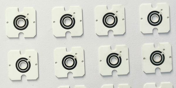
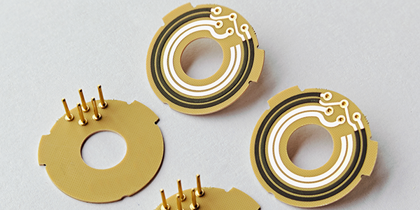
Potentiometer Taper PCB
Potentiometer Taper PCBs are specially designed printed circuit boards that integrate the functionality of taper potentiometers, with the primary function of providing a nonlinear resistance change based on the rotational angle, allowing precise control over voltage or current, enabling the potentiometer to achieve specific voltage or current adjustment effects at different positions, making them widely used in applications requiring precise voltage or current control such as audio equalizers, sensor readings, precision measuring equipment, and industrial control systems.
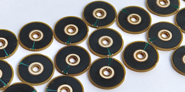
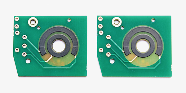
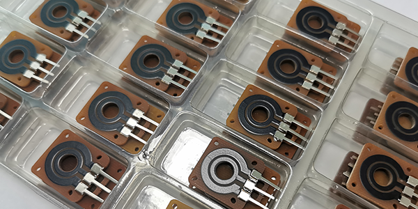
Potentiometer Taper PCBs are manufactured using thick-film resistor technology. Nonlinear resistive materials are printed onto insulating substrates like FR4 or ceramic, followed by a sintering process to create thick-film resistors. This process ensures the electrical performance and reliability of the potentiometer, particularly in applications that demand high precision and stability. The thick-film resistor manufacturing technique enables precise resistance adjustment in a compact space, reducing the size and enhancing the integration of the product.
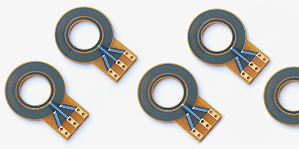
Potentiometer Taper PCBs have the unique feature of multi-segment nonlinear resistance change, which allows precise voltage or current adjustment during operation. The resistance change follows a nonlinear relationship with the rotational angle, making them suitable for applications that require nonlinear adjustment. Compared to traditional potentiometers, the taper potentiometer design not only makes the circuit board more compact but also reduces the need for external components, increasing the integration of the product. Furthermore, their stability and long lifespan make them ideal for high-precision control systems.
Potentiometer Taper PCBs are widely used in various fields requiring precise voltage or current control. They are commonly used in audio equalizers to adjust the intensity and quality of audio signals, ensuring balance and optimization of different frequency ranges. In sensor readings and precision measuring equipment, they provide accurate voltage variations, ensuring the accuracy of data collection. In industrial control systems, Potentiometer Taper PCBs are used to adjust and control machine operations, keeping various parameters within the ideal range, thereby improving the accuracy and stability of the equipment.
Advantages of Potentiometer Taper PCB :
● Nonlinear Resistance Control: Potentiometer Taper PCBs offer precise nonlinear resistance changes based on rotational angle. This allows for finer and more accurate voltage or current adjustments, which are critical in applications such as audio equalizers, industrial controls, and precision measuring equipment.
● Compact Design: The integration of taper potentiometers directly onto the printed circuit board (PCB) reduces the overall size of the component. This makes them suitable for space-constrained applications and reduces the need for additional external components, improving overall system efficiency.
● Improved Integration: Potentiometer Taper PCBs streamline the design by combining multiple functions into one compact unit, improving circuit board integration and simplifying assembly processes. This increases the reliability and reduces manufacturing complexity.
● Durability and Longevity: These PCBs are designed to last longer due to the robustness of the thick-film resistor technology used in their production. They can withstand high temperatures and harsh environments, ensuring reliability and stability over extended usage periods.
● High Precision: With the use of thick-film resistor technology, Potentiometer Taper PCBs can provide highly accurate resistance values, making them ideal for high-precision applications where fine control of voltage or current is necessary, such as in laboratory instruments or high-end audio equipment.
● Versatile Applications: Potentiometer Taper PCBs are suitable for a wide range of industries and applications, including audio equipment, sensor systems, industrial controls, and precise measurement devices, due to their versatile nature and ability to offer fine-tuned resistance adjustments.
Manufacturing Processes of Potentiometer Taper PCB :
● Substrate Preparation: The substrate for Potentiometer Taper PCBs are typically made from materials such as FR4, flexible polyimide (PI), alumina (Al2O3), aluminum nitride (AlN). These substrates undergo laser etching, shaping, and drilling processes to form the initial structure of the potentiometer. The choice of substrate significantly impacts the performance of the potentiometer, as it must exhibit excellent electrical insulation and mechanical strength.
● Thick Film Resistor Printing: The preparation of thick film resistor paste is one of the critical steps. This carbon paste is generally composed of conductive materials, glass beads, and organic solvents. It is accurately printed onto the substrate using screen printing technology, creating the resistive pathways. After printing, the paste is dried and subjected to high-temperature sintering to solidify the resistor layer and achieve the desired resistance value.
● Laser Trimming: Once the sintering process is complete, the resistor's substrate is trimmed to achieve precise resistance values in a step known as laser trimming. This method allows for highly accurate adjustments to the resistance, ensuring the potentiometer's precision and stability.
● Protective Layer Printing: To protect the resistor layer from subsequent processes, such as laser trimming, and to provide long-term environmental protection, one or more protective layers are printed over the resistor layer. These protective layers are typically made from glass materials and require drying and sintering.
● Connection of End and Intermediate Electrodes: The end electrodes connect the surface electrodes to the back electrodes, ensuring the electrical connection of the resistor body to the resistor pins. The intermediate electrodes are formed using nickel sputtering technology to create side conductors that isolate the internal silver electrodes and prevent oxidation.
● External Electrode Plating: To enhance the solderability and manufacturability of the resistor, a layer of metal, usually tin, is plated onto the external electrodes. This step improves the connection performance and reliability of the resistor.
● Quality Inspection and Testing: In the later stages of production, the resistors undergo various quality control processes, including particle inspection, magnetic sorting, electrical performance testing, and tape packaging, to ensure that the final product meets quality standards.
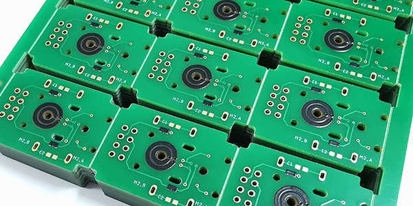
● PCB Layout and Manufacturing: The manufacturing of Potentiometers Taper PCBs also includes PCB layout design, material selection, inner layer fabrication, ultraviolet exposure, removal of unwanted copper, lamination, drilling, and electroplating. These steps ensure that the PCB's circuit design is precise and that the connections between different layers are strong and reliable.
The entire manufacturing process requires precise control and high-quality materials to ensure that the Potentiometers Taper PCBs meet the demands for accuracy in control applications.
Potentiometer Taper PCB in Audio Equipments :
● Volume Control: Potentiometer Taper PCBs are widely used for volume control in audio devices. Since human perception of sound intensity follows a logarithmic scale, the nonlinear taper of these potentiometers provides more natural and precise adjustments from very quiet to very loud. This ensures that users can fine-tune the loudness with ease, improving the overall audio experience.
● Audio Signal Processing: In audio devices like amplifiers or mixers, Potentiometer Taper PCBs are used to adjust the gain of audio signals. By altering the resistance in the audio signal path, these PCBs offer accurate control over signal strength, enabling precise amplification or attenuation, which is essential for optimal sound processing.
● Audio Equalization: Potentiometer Taper PCBs are essential in audio equalizers, where they help adjust the gain of specific frequency bands. This ability to enhance or attenuate certain frequencies allows audio engineers or users to shape the sound to their preference, ensuring the best possible sound quality for different listening environments.
● Digital Potentiometer Applications: In digital audio devices, digital potentiometers on Potentiometer Taper PCBs provide precise control over volume and audio balance. These digital potentiometers typically feature nonlinear tapers, with each step corresponding to a 1 dB change, allowing for accurate and repeatable adjustments in digital audio processing.
● Zero-Cross Detection Feature: To reduce noise during volume adjustments, some digital potentiometers incorporate zero-cross detection. This ensures that the potentiometer's position changes only when the audio signal crosses zero, thus minimizing unwanted noise and providing a cleaner audio output during adjustments.
● Multichannel Audio Devices: In multichannel audio systems like stereo or surround sound setups, Potentiometer Taper PCBs can be used to control the volume of individual channels or multiple channels simultaneously. This feature is crucial for achieving balanced sound across various audio sources, enhancing the user's experience by ensuring consistent audio levels.
● Precise Control of Audio Signals: In more advanced audio devices such as digital mixing consoles, amplifiers, and other audio adjustment tools, Potentiometer Taper PCBs enable precise control of audio signals. With their ability to fine-tune sound levels digitally, they offer users highly detailed and responsive control, which is essential in professional audio applications.
Process Capabilities of Potentiometer PCB :
Items |
Typical Values |
1, Substrates : |
FR4, Alumina (Ceramic), Polyimide (Flexible PCB), Stainless Steel (SUS304), Mica |
2, Conductors Material : |
Copper, Silver , Gold , Silver-Palladium, Palladium-Gold |
3, Thick Film Carbon Thickness (height) : |
15um +/-5 um |
4, Silver Palladium Thickness (height) : |
12um+/-5um |
5, Minimum Width of Thick Film Traces : |
0.25 mm +/-0.05 mm |
6, Minimum Spacing of Thick Film Traces : |
0.25 mm +/-0.05 mm |
7, Minimum Footprint (Carbon to Copper) : |
No less than 0.20mm |
8, Sheet Resistivity (ohms/square): |
Printed resistors in milli ohm to mega ohm range (Customizable) with tolerances of 1-10% are fabricated and protected with overglaze materials |
9, Resistor Value Tolerance : |
+/-10.0% (Standard) (Customizable) |
10, Linearity : |
+/-1.0% (Standard) (Customizable) |
11, Synchronism of Potentiometers (Double Channels) : |
+/-2.0% (Standard) (Customizable) |
12, Durability of Carbon Ink (Life time) : |
0.5 Million (Min), 2.0-5.0 Million (Standard) |
13, Working Temperature : |
- 40℃ /+150℃ |
For more information, Please refer to Thick Film Potentiometer PCB.
Custom Thick Film Sensors
- Custom Thick Film Sensor Elements
- Fuel Level Sensor PCB
- Fuel Level Sensor Ceramic PCB
- Oil Level Sensor Ceramic PCB
- Motorcycle Fuel Level Sensor PCB
- Throttle Position Sensor PCB
- Throttle Position Sensor FR4 PCB
- Throttle Position Sensor Ceramic PCB
- Throttle Position Sensor Flexible PCB
- Accelerator Pedal Sensor PCB
- Accelerator Pedal Position Sensor PCB
- Pedal Position Sensor Carbon PCB
- Potentiometer PCB
- Linear Potentiometer Carbon Track PCB
- Rotary Potentiometer Carbon Track PCB
- FR4 Potentiometer Carbon PCB
- Ceramic Potentiometer Carbon PCB
- Flexible Potentiometer Carbon PCB
- Logarithmic Taper Potentiometer PCB
- Position Sensor PCB
- FR4 Position Sensor Carbon PCB
- Ceramic Position Sensor Carbon PCB
- Flexible Position Sensor Carbon PCB
- Flexible Sensor PCB
- Printed Flexible Electronic PCB
- Printed Carbon PCB
- Ceramic Pressure Sensors
- Ceramic Thick Film Pressure Sensors
- Engine Oil Pressure Sensor PCB
- Gold Coated Ceramic Substrates
- Gold Coated Thick Film Substrates
- Metallized Ceramic Substrates
- Multilayer Thick Film Substrates
- Thick Film Metallization Technology
- Thin Film Metallization Technology
- Thin Film Ceramic PCB
- Variable Resistor Carbon PCB
- Remote Ready Sender Ceramic PCB
- LP Gas Tank Gauges Ceramic PCB
- Thick Film Capacitive Sensors
- Thick Film Capacitive Pressure Sensors
- Thick Film Edible Oil Quality Sensors
- Thick Film Meteorological Rainfall Sensors
- PI Interdigital Electrodes (Flexible)
- Air Door Actuator PCB
- HVAC Blend Door Actuator PCB