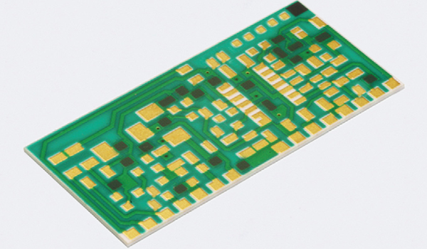
Thick Film Gold Multilayer Substrates
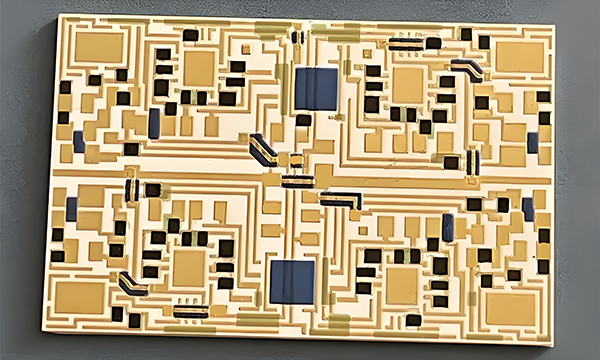
Thick Film Gold Multilayer Substrates, also called Multilayer Gold Thick Film Substrates, are produced using advanced thick film technology that precisely integrates conductive materials (typically gold) with dielectric layers to form a robust circuitry path, with gold layers typically applied to the ceramic substrate through screen printing or sputtering techniques, allowing for precise placement of conductive and resistive materials to ensure efficient electrical connections and signal transmission in complex circuits.
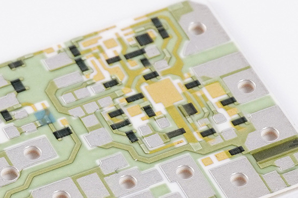
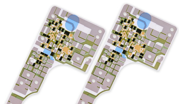
Thick Film Gold Multilayer Substrates feature excellent conductivity, corrosion resistance, and superior thermal stability. Gold, as a conductive material, enhances the reliability and longevity of electronic components. The multilayer structure enables these substrates to support more circuit layers while maintaining high electrical performance. Furthermore, their ceramic substrate provides additional mechanical strength and high-temperature resistance, making them ideal for high-frequency circuits and hybrid microelectronics.
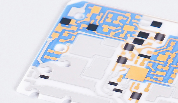
Multilayer Gold Thick Film Substrates are widely used in the electronics field, particularly in high-frequency circuits and hybrid microelectronics, serving as a base platform for connecting and supporting various electronic components. These substrates are commonly found in wireless communications, automotive electronics, military equipment, and other applications requiring high precision and stability in signal transmission. Their multilayer structure and metallic conductive properties provide significant advantages in complex electronic applications.
Features of Thick Film Gold Multilayer Substrates :
Thick Film Gold Multilayer Substrates are engineered for high-performance, offering a combination of durability, precision, and versatility in demanding electronic applications. Key features include:
● Multiple Metal Layers:
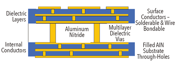
Typically consisting of 4 to 6 metal layers, including ground planes and hermetic plugged vias, which ensure better signal routing, isolation, and improved reliability.
● Excellent Wire Bondability and Solderability:
The gold layers provide superior wire bondability, solderability, and conductor adhesion, ensuring stable, high-quality electrical connections in high-density circuits.
● Dielectric Insulation and Adjustable Dielectric Constant:
These substrates offer 1,000-volt insulation and an adjustable dielectric constant ranging from 6 to 12, making them adaptable for different electrical needs and high-frequency applications.
● Printed Resistors with Overglaze Protection:
Incorporating printed resistors with 1%-10% tolerances, these are typically protected with overglaze materials, ensuring durability against environmental factors and providing long-term stability.
● Superior Conductivity:
Gold is an excellent conductor, minimizing resistance and signal loss, which is essential for high-speed, high-frequency circuit designs.
● Corrosion Resistance:
Gold's natural resistance to oxidation and corrosion makes these substrates ideal for harsh environments, ensuring a longer lifespan for the electronic components.
● Thermal Stability:
Gold maintains its properties over a wide temperature range, ensuring reliable performance in high-temperature applications and maintaining stability under thermal stress.
Manufacturing of Thick Film Gold Multilayer Substrates :
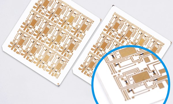
Thick Film Gold Multilayer Substrates are produced through state-of-the-art equipment and processes, including automated cassette-to-cassette screen printing and firing, high-speed laser trimming, photolithography, and dicing.
● Substrate Preparation: The process starts with a ceramic substrate, typically made of materials such as alumina or other ceramics, which provides mechanical strength and thermal stability. The substrate is cleaned and prepared for the application of thick film materials.
● Screen Printing: Conductive materials, often gold, are applied onto the ceramic substrate using a screen printing technique. This allows for precise placement of gold layers, which will form the electrical pathways. Gold is selected due to its excellent conductivity and resistance to corrosion.
● Firing: After screen printing, the substrate is fired in a high-temperature furnace to sinter the gold and dielectric materials, ensuring a strong bond to the ceramic substrate. The firing process also helps in the creation of the necessary electrical and mechanical properties.
● Layering: In the case of multilayer substrates, additional layers of conductive and dielectric materials are applied using successive screen printing and firing cycles. Each layer is carefully aligned to ensure proper electrical connections between different circuit elements.
● High-speed Laser Trimming: Once the layers are applied and fired, excess material may be removed using a high-speed laser trimming process. This step ensures that the final substrate matches the precise design specifications and eliminates any imperfections in the circuit layout.
● Photolithography and Dicing: Photolithography techniques are used to define the intricate patterns of the circuitry. A photoresist layer is applied, exposed to light, and developed to create the desired pattern on the substrate. Afterward, the substrate is diced into individual units using precision cutting techniques.
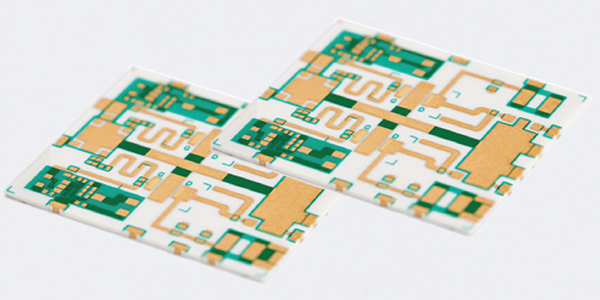
Applications of Multilayer Gold Thick Film Substrates :
Multilayer Gold Thick Film Substrates are widely used in various demanding electronic fields, particularly suitable for high-density electronic applications, offering a perfect balance of economy, performance, and reliability. Below are the main areas of application:
● High-Frequency Circuits: Used in RF and microwave circuits, where signal integrity is crucial.
● Hybrid Microelectronics: Employed in systems that combine different types of electronic components on a single substrate.
● Aerospace and Defense: Chosen for its reliability and durability in extreme environments, making it ideal for aerospace and defense applications.
● Telecommunications: Utilized in high-speed data transmission systems, where low signal loss is essential.
● Automotive Electronics: Applied in automotive electronic control systems, such as engine control units, sensors, and infotainment systems. These substrates can withstand high temperatures, vibrations, and electrical noise while providing stable performance.
● Medical Devices: Used in diagnostic equipment, implantable devices, and medical sensors, ensuring high reliability and precision in demanding environments.
● Power Electronics: Employed in power electronics applications like power amplifiers and voltage regulators, providing high efficiency and reliability, ideal for environments requiring high current and heat dissipation.
● Consumer Electronics: Used in consumer electronics like smartphones, wearable devices, and high-performance audio systems, enabling compact designs and high signal integrity.
● Photovoltaics (Solar Energy): Used in solar inverters and other power management circuits, ensuring long-term reliability and performance in outdoor environments.
● Radio Frequency Identification (RFID): Applied in RFID technology, particularly in tags and readers, where they operate efficiently in high-frequency systems with minimal signal loss.
● Test and Measurement Equipment: Employed in test and measurement equipment, providing precision and high-frequency performance to ensure accurate measurements and data collection.
Advantages of Multilayer Gold Thick Film Substrates :
Multilayer Gold Thick Film Substrates are used in advanced electronic and microelectronic applications, offering a range of advantages due to the unique properties of gold and the structure of multilayer substrates. Some of the key advantages include:
1. Excellent Electrical Conductivity:
● Superior Conductivity: Gold is an excellent conductor of electricity, which makes it ideal for high-performance applications where minimal resistance is required. The use of thick gold films ensures low electrical resistance and stable performance even under high-frequency or high-power conditions.
● Stable Performance: Gold does not oxidize or corrode easily, maintaining consistent electrical conductivity over time, even in harsh environments.
2. High Reliability and Durability:
● Corrosion Resistance: Gold is highly resistant to corrosion and oxidation, making it particularly useful in environments where moisture or chemicals might degrade other materials. This property ensures that the gold layers on the substrate maintain their performance and integrity over long periods.
Longevity: The stability of gold under high temperature and humidity, coupled with its resistance to tarnishing, ensures that multilayer gold thick film substrates offer long-term durability and reliability, even in extreme conditions.
3. Thermal Stability:
● Good Thermal Conductivity: Gold has excellent thermal conductivity, which helps in dissipating heat efficiently from high-power components. This makes multilayer gold substrates suitable for applications in power electronics, where thermal management is crucial.
● Thermal Resistance to Oxidation: Unlike other metals like copper or silver, gold does not oxidize or form conductive oxides that could interfere with the performance of the substrate, thus ensuring consistent thermal properties over time.
4. Enhanced Mechanical Strength and Integrity:
● Improved Structural Integrity: Multilayer substrates typically offer better mechanical strength and stability compared to single-layer substrates. The combination of multiple layers allows for optimized stress distribution, improving the overall mechanical integrity of the substrate.
● Resistance to Mechanical Stress: Gold's inherent malleability allows it to withstand some degree of mechanical stress without cracking or delaminating, making it suitable for applications where the substrate might be subjected to physical forces or vibration.
5. Flexibility in Design and Functionality:
● Multilayer Design for Complexity: Multilayer substrates allow for more complex designs with different functional layers, such as conductive, insulating, and adhesive layers, all within a single substrate. This enables designers to integrate multiple functionalities, reducing the need for separate components and simplifying the overall system design.
● Customization: The ability to stack multiple layers with different materials provides significant flexibility in tailoring the substrate’s properties (e.g., electrical, thermal, and mechanical) to meet the specific needs of an application.
6. Solderability and Bonding:
● Excellent Solderability: Gold is highly solderable, making it ideal for use in electronic assemblies. It forms reliable and low-resistance solder joints, ensuring stable connections in high-performance circuits.
● Reliable Interconnects: Gold is used in many microelectronic applications for making reliable interconnects between components. It provides a stable, low-resistance bond that can withstand the mechanical stresses and thermal cycles common in electronic assemblies.
7. High Frequency and Low Signal Loss:
● Low Signal Loss: Because of its low electrical resistance, gold is particularly advantageous in high-frequency applications. Multilayer gold substrates can provide minimal signal loss, making them ideal for use in RF (radio frequency) and microwave circuits, where signal integrity is critical.
● High Frequency Stability: Gold maintains its properties at high frequencies, ensuring that signal transmission remains stable even in systems operating at GHz frequencies.
Challenges of Thick Film Gold Multilayer Substrates :
Thick Film Gold Multilayer Substrates are commonly used in various high-performance electronic applications, such as in microelectronics, automotive electronics, and telecommunications, where reliability and performance are crucial. However, there are several challenges associated with designing and manufacturing thick film gold multilayer substrates:
1. Cost and Material Challenges:
● Gold is Expensive: Gold is a precious metal, and using it in thick film form can increase the overall cost of the substrate significantly. For applications where large quantities of substrates are needed, this cost can be a major concern.
● Material Consumption: The amount of gold used in thick film printing is higher compared to thinner films or other metals, which can further raise costs.
2. Thermal Expansion Mismatch:
● Coefficient of Thermal Expansion (CTE) Mismatch: Gold has a relatively low coefficient of thermal expansion (CTE), and this can be mismatched with other materials in the multilayer structure (such as ceramic or copper layers). This mismatch can lead to stress and potential delamination, warping, or cracking of the substrate during thermal cycling.
● Thermal Stability: Gold can soften at higher temperatures, which could compromise the mechanical stability of the multilayer structure under thermal cycling conditions, especially in high-temperature environments.
3. Mechanical Strength:
● Low Hardness of Gold: Pure gold is relatively soft and can be prone to deformation under mechanical stress. This could cause issues such as warping or cracking, particularly in high-stress areas or in applications where the substrate is subjected to mechanical loads during operation.
● Brittleness of Multilayer Structures: As the number of layers in the multilayer structure increases, the likelihood of interfacial failure or brittle fracture increases, especially when thermal or mechanical stresses are applied.
4. Fabrication Challenges:
● Layer Adhesion: Achieving strong adhesion between gold and other layers, such as ceramic or other metal layers, can be challenging. This often requires specialized deposition techniques, such as sputtering, electroplating, or screen printing, which must be carefully controlled to ensure good adhesion and prevent delamination.
● Complex Processing: The fabrication of thick film multilayer substrates often involves multiple printing steps, each of which requires precise control. The process can be time-consuming and susceptible to defects, leading to yield loss.
● Inconsistency in Layer Thickness: Achieving consistent and uniform thickness in each layer of the gold film can be difficult, particularly when working with thick films. Variations in thickness can affect the performance of the substrate, including its electrical conductivity and thermal characteristics.
5. Electrical Performance:
● Surface Oxidation: Gold can form a thin oxide layer on its surface when exposed to air, which can affect its electrical conductivity. Although gold is resistant to corrosion, oxidation can still reduce its effectiveness in certain applications, particularly in microelectronics, where low resistance and high conductivity are essential.
● Contact Resistance: The quality of the metal-to-metal or metal-to-solder interfaces can impact the overall electrical performance. If the gold layer is not properly prepared or if there are imperfections in the interface, it could result in increased contact resistance or unreliable electrical connections.
For more information, Please refer to Thick Film Substrates.
Custom Thick Film Sensors
- Custom Thick Film Sensor Elements
- Fuel Level Sensor PCB
- Fuel Level Sensor Ceramic PCB
- Oil Level Sensor Ceramic PCB
- Motorcycle Fuel Level Sensor PCB
- Throttle Position Sensor PCB
- Throttle Position Sensor FR4 PCB
- Throttle Position Sensor Ceramic PCB
- Throttle Position Sensor Flexible PCB
- Accelerator Pedal Sensor PCB
- Accelerator Pedal Position Sensor PCB
- Pedal Position Sensor Carbon PCB
- Potentiometer PCB
- Linear Potentiometer Carbon Track PCB
- Rotary Potentiometer Carbon Track PCB
- FR4 Potentiometer Carbon PCB
- Ceramic Potentiometer Carbon PCB
- Flexible Potentiometer Carbon PCB
- Logarithmic Taper Potentiometer PCB
- Position Sensor PCB
- FR4 Position Sensor Carbon PCB
- Ceramic Position Sensor Carbon PCB
- Flexible Position Sensor Carbon PCB
- Flexible Sensor PCB
- Printed Flexible Electronic PCB
- Printed Carbon PCB
- Ceramic Pressure Sensors
- Ceramic Thick Film Pressure Sensors
- Engine Oil Pressure Sensor PCB
- Gold Coated Ceramic Substrates
- Gold Coated Thick Film Substrates
- Metallized Ceramic Substrates
- Multilayer Thick Film Substrates
- Thick Film Metallization Technology
- Thin Film Metallization Technology
- Thin Film Ceramic PCB
- Variable Resistor Carbon PCB
- Remote Ready Sender Ceramic PCB
- LP Gas Tank Gauges Ceramic PCB
- Thick Film Capacitive Sensors
- Thick Film Capacitive Pressure Sensors
- Thick Film Edible Oil Quality Sensors
- Thick Film Meteorological Rainfall Sensors
- PI Interdigital Electrodes (Flexible)
- Air Door Actuator PCB
- HVAC Blend Door Actuator PCB